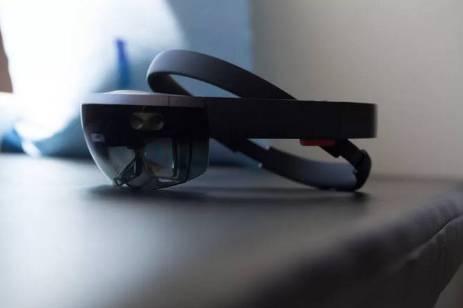
Since the release of the HoloLens developer version, Microsoft has been secretly keeping details of its special Holographic Processing Unit. At this week's Hot Chips 2016 conference, Microsoft finally retired, unraveling the mystery of the HPU chip.
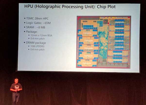
According to Nick Baker, Microsoft's equipment engineer, the HPU chip is a custom chip that handles data transfer between the CPU and the camera and different sensors. It uses the TSMC TSMC foundry 28nm process technology, with up to 24 Tensilica DSP (digital signal processing) core, can handle 1 trillion instructions per second, while equipped with 8MB SRAM, 1GB LPDDR3 memory.
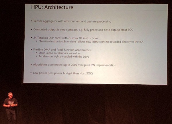
In addition, the HPU chip also uses a 12x12mm BGA package. Compared with the software solution, the HPU increases the data transmission rate by 200 times and the power is only 10W. Low power consumption and high efficiency are mainly due to Microsoft's use of the Tensilica instruction extension to add 10 custom instructions to speed up the speed required by HoloLens and the data provided by Intel Atom, reducing the computational effort of the Atom x86 Cherry Trail processor.
Therefore, the production of complex HPU chips is also one of the main reasons that HoloLens has not been able to produce in batches. However, Microsoft has now developed and purchased for developers in North America, each user can purchase five devices, the price is still familiar with 3,000 US dollars.