In order to facilitate production, PCB circuit board imposition generally needs to design Mark points, V-grooves, and process edges.
First, the imposition shape1. The outer frame (clamping edge) of the PCB panel should adopt a closed-loop design to ensure that the PCB panel will not be deformed after it is fixed on the fixture.
2, PCB board width ≤ 260mm (SIEMENS line) or ≤ 300mm (FUJI line); if you need automatic dispensing, PCB board width & TImes; length ≤ 125 mm & TImes; 180 mm.
3, PCB layout as close to the square as possible, it is recommended to use 2 & TImes; 2, 3 & TImes; 3, ... puzzle; but do not spell into a yin and yang;
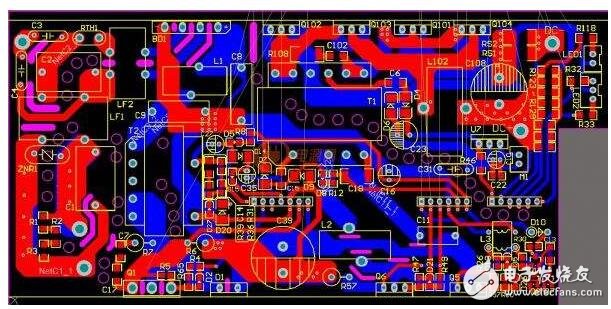
1. After opening the V-groove, the remaining thickness X should be (1/4 to 1/3) plate thickness L, but the minimum thickness X must be ≥ 0.4 mm. The upper limit of the board with heavier load can be taken, and the lower limit can be taken for the board with lighter load.
2. The misalignment S of the upper and lower sides of the V-shaped groove should be less than 0.1mm; due to the limitation of the minimum effective thickness, the V-grooved plate method should not be adopted for the plate with the thickness less than 1.2mm.
1. When setting the reference positioning point, usually leave a non-resistance area 1.5 mm larger than the positioning point.
2, used to help the optical positioning of the placement machine PCB board with a patch device at least two asymmetric reference points diagonally (http:// copyright) the entire PCB optical positioning reference point is generally in the whole PCB Diagonal corresponding position; the reference point for optical positioning of the block PCB is generally at the corresponding position of the diagonal PCB circuit board.
3. For QFP (square flat package) with lead pitch ≤ 0.5mm and BGA (ball grid array package) with ball pitch ≤ 0.8mm, in order to improve the placement accuracy, it is required to set the reference point at two diagonals of the IC.

1. There should be no large devices or protruding devices near the connection point between the outer frame of the panel and the inner small plate, small plate and small plate, and the space between the components and the PCB circuit board should be more than 0.5mm. To ensure the normal operation of the cutting tool.
Five, the board positioning hole1. The whole board positioning for PCB circuit board and the reference symbol for fine pitch device positioning. In principle, the QFP with a pitch less than 0.65mm should be set at its diagonal position; the positioning reference symbol for the imposition PCB sub-board should be Used in pairs, placed at the opposite corner of the positioning feature.
2, large components should be left with positioning posts or positioning holes, such as I / O interface, microphone, battery interface, micro switch, headphone interface, motor and so on.
A good PCB designer should consider the factors of production when making imposition design, so as to facilitate processing, improve production efficiency and reduce production cost.

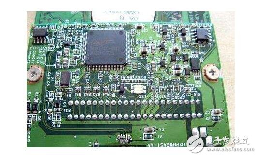
The rational layout of PCB circuit board components in chip processing is the basic premise for designing high quality PCB drawings. The requirements for component layout mainly include five aspects of installation, stress, heat, signal and appearance.
1, installationRefers to a series of basic requirements for the installation of the board into the chassis, the enclosure, and the slot in a specific application without causing interference such as space interference or short circuit, and placing the specified connector in a specified position on the chassis or the casing. Claim.
2, stressedThe circuit board in the chip processing should be able to withstand various external forces and vibrations during installation and operation. For this reason, the circuit board should have a reasonable shape, and the positions of various holes (screw holes, shaped holes) on the board should be reasonably arranged. Generally, the distance between the hole and the edge of the plate is at least greater than the diameter of the hole. At the same time, it should be noted that the weakest section of the plate caused by the shaped hole should also have sufficient bending strength. The connector that directly “extends†the device from the board should be reasonably fixed to ensure the reliability of long-term use.
3, heatedFor high-power, severely heated devices, besides ensuring heat dissipation conditions, be careful to place them in the proper position. Especially in sophisticated analog systems, special attention should be paid to the adverse effects of the temperature field generated by these devices on the fragile preamplifier circuit. Generally, the part with very large power should be made into a single module and take certain thermal isolation measures from the signal processing circuit.
4, the signalSignal interference is the most important factor to consider in PCB board layout design. The most basic aspects are: weak signal circuit and strong signal circuit are separated or even isolated; AC part is separated from DC part; high frequency part is separated from low frequency part; pay attention to the direction of signal line; ground line arrangement; proper shielding and filtering And other measures.
5, beautifulNot only must we consider the neatness of the placement of components, but also consider the graceful flow of the traces. Since the average layman sometimes emphasizes the former, to evaluate the advantages and disadvantages of the circuit design one-sidedly, for the image of the product, the former should be given priority when the performance requirements are not critical. However, in high-performance applications, if you have to use a double-panel, and the board is also packaged inside, you can't see it normally, you should give priority to the aesthetics of the trace.
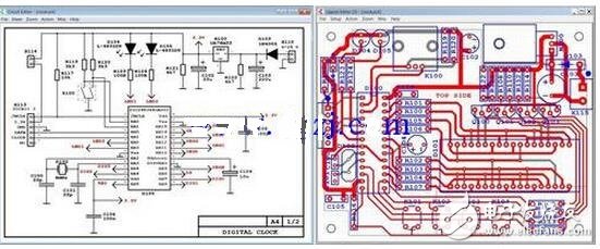
What software can PCB draw in addition to DXP?The first on our list is the ZentiPCB platform from Mirko Bruno Sortini, which offers a range of free software to help users design their own PCBs. ZentiCapture allows users to quickly and easily design schematics using a simple tool set that allows users to place parts (component symbols) through orthogonal locking and pin snapping. Once the schematics (in the form of a chart) are completed, they can be ported to ZentiPCb.
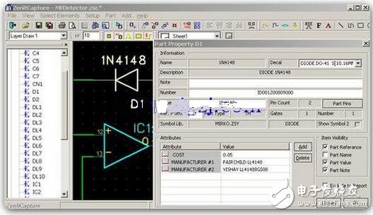
ZentiPCB is a CAD-based program that allows users to import netlist files and visualize their charts. The layout editor provides the ability to import components directly from the library using cursors, supporting single-sided and dual-panel depending on the requirements.
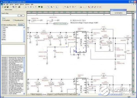
TinyCAD comes from SourceForge users beuscher, don_lucas and mattpyne. Don't underestimate the software because of the name of the software. This software provides all the features of PCB design and layout design. The software contains 42 libraries with a total of 755 symbols, including digital logic gates, electromechanical components and even microcontrollers. And each of these components can be edited, and users can even add their own component symbols. TinyCAD supports a variety of netlist formats (Eagle SCR, PADS-PCB, XML, etc.), as well as SPICE netlists.
CometCAD is an excellent example of another free software platform that provides an electronic schematic editor and a PCB layout editor. Only this software only supports the Windows platform. The CometCAD electronic schematic editor supports multi-page schematics, symbol rotation, parts lists and netlist schematic outputs. The PCB Layout Editor provides almost all of the functions mentioned previously (component libraries, double-sided PCBs, etc.), as well as the ability to output CAM files, as well as the ability to design rectangular multi-PCB boards.
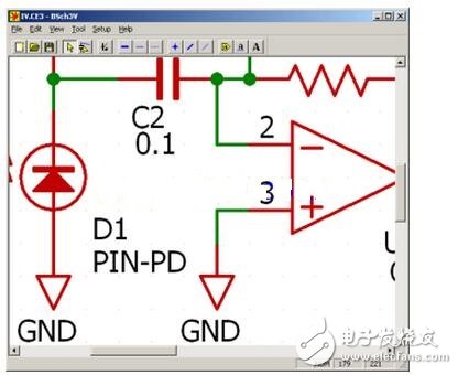
Those who don't want unnecessary functionality and only need the most basic functions can try Suigyodo's BSch3V schematic capture package (where BSch stands for Basic Schematic basic schematic). The PCB editor allows users to design single-layer, double-layer, or even four-layer PCB boards with a design area of ​​30 square millimeters. It also has a component library, a component list generator, and a netlist generator. Users can also use the other two software to enhance the BSch3V's capabilities, including SmdICpad (for QFP, PLCC, SOP data) and POLYGON (copper-placed area).
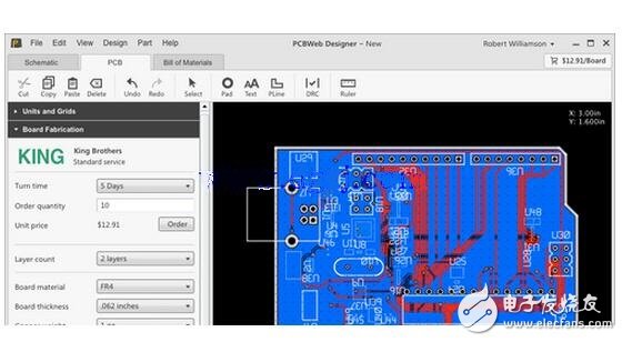
PCWeb's Designer is one of the most feature-rich editors on the web and is free to use. The software has an impressive lineup of tools including Schematic Capture (placement components, routing/networking, annotations, etc.), PCB (placement components, routing, design rule checking, etc.) and Part Editor (create/definition components, add Symbols, etc.), in addition to the BOM function, the BOM Manager integrates Digi-Key, allowing users to assign a number to each individual component on their PCB, which will be displayed through the BOM to facilitate procurement. . This software is a software that is efficient for efficient production.
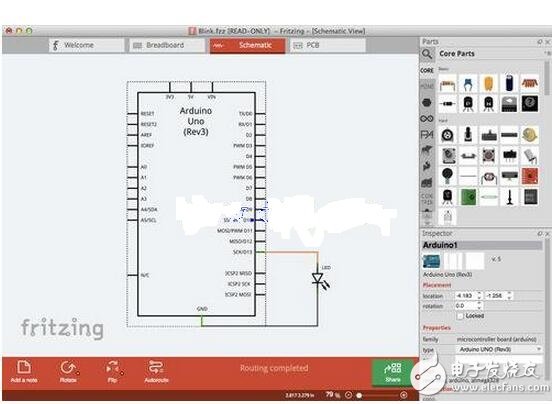
The Fritzing platform is more than just a simple PCB editor, but its purpose is to actually create its own designs for makers and hackers. It is designed to allow users to implement their own Arduino-based microcontroller design and create PCB layouts that can be used for production. Once the user has designed an actual circuit on the breadboard, it can then be transferred to the editor, which contains three different project perspectives. The breadboard perspective allows the user to drag and place virtual electronic components on a virtual breadboard. The schematic view is the formal expression of the schematic, which is the correspondence of the circuits on the virtual breadboard, but the user can also edit as needed. Finally, the PCB viewing angle allows the user to place the component on a virtual printed circuit board and then use it for production.

One of the most popular PCB free editors on the Internet is KiCAD, an EDA tool similar to Fritzing above. The software provides the functionality of a virtual environment at every stage of the design process. Among the components included are Eeschema (schematic editor), Pcbnew (printed circuit board editor), Gerbview (Gerber file viewer), and Cvpcb (for component association path selector). There is also a built-in BOM manager that allows users to tag bills of materials and easily calculate costs.
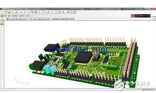
DesignSpark's PCB platform is another PCB editing tool for widely used EDA applications. Similar to the two tools mentioned above, DesignSpark PCB provides schematic editing, while PCB Wizard is used to complete the schematic, and Autorouter can automate the routing between components. However, the software does have some points to pay attention to. For example, this software is very resource-intensive. If the project does not exist on the same computer, problems may occur. In addition, some functions must be registered before the user can be unlocked, and the worst is The software also displays ads.
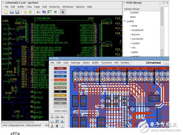
Despite the fact that most of the PCB software runs on Windows-based computers, some are designed for Linux users, including Ales Hvezda's gEDA project, which provides a collaborative open source EDA tool. The collaborative part refers to the continuous efforts of developers working together to develop and update the gEDA toolkit, including gEDA schematic capture and circuit design for the netlist platform, PCB layout design and optimization, and Icarus Verilog (a type of simulation Hardware description language for electronic systems). It also includes ngspice/ngucap SPICE/simulator, gerbv Gerber viewer and GTKWave digital waveform viewer.
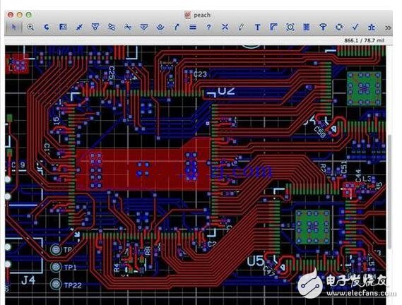
A PCB editor for Mac comes from Osmand PCB, which allows the user to do PCB designs of almost any size, shape, and how many layers to make. The software can be designed for wiring up to 10 nanometers in spatial resolution and at any angle, and supports both imperial and metric units. Osmand also allows users to move and relocate components, connect/route/modify paths, and design PCB labels using the libraries they contain. The software also supports scripting support for the Lua language, which can generate Gerber (RS-274X) files and Excellon presentation files. This is a luxury configuration for a free software.

ECU Connector Section.
ECU-MEM-CONNECTOR is used to connect the ECU-MEM to the DIAG-LAYER. This part of ODX also links the ECU-MEM-objects with DIAG-COMMS e.g. used to read idents, download or upload the data. It allows an ECU to be flashed using ODX.
There are nearly 100 kinds of connectors used in general automobiles, and hundreds of connectors are used in a single vehicle model. With the increasing demand for automobile safety, environmental protection, comfort and intelligence, the application of automotive electronic products is increasing, which will make the number of Automotive Connector applications increase.
Four basic structural components of automobile connector
1. Contact
It is the core part of automobile connector to complete the electrical connection function. Generally, the contact pair is composed of positive contact and negative contact, and the electrical connection is completed by inserting the female and male contacts. The positive contact is a rigid part, and its shape is cylindrical (round pin), square cylinder (square pin) or flat (insert piece). The positive contact is generally made of brass and phosphor bronze.
The female contact, namely jack, is the key part of the contact pair. It relies on the elastic structure to produce elastic force due to elastic deformation when it is inserted with the pin, and forms a close contact with the positive contact to complete the connection. There are many kinds of Jack structures, such as cylinder type (split slot, shrink mouth), tuning fork type, cantilever beam type (longitudinal slot, 9-shaped), box type (square socket) and hyperboloid linear spring jack.
2. Shell
Also known as the shell, it is the cover of automobile connector, which provides mechanical protection for the built-in insulation mounting plate and pin, and provides the alignment of plug and socket when inserting, so as to fix the connector to the equipment.
3. Insulator
Insulator is also called automobile connector base or insert. Its function is to arrange the contact according to the required position and spacing, and to ensure the insulation performance between contacts and between contact and shell. Good insulation resistance, voltage resistance and machinability are the basic requirements for selecting insulating materials to be processed into insulators.
4. Annex
Accessories are divided into structural accessories and installation accessories. Structural accessories such as snap ring, locating key, locating pin, guide pin, connecting ring, cable clamp, sealing ring, sealing gasket, etc. Install accessories such as screws, nuts, screws, coils, etc. Most accessories have standard parts and general parts. It is these four basic structural components that enable the automotive connector to act as a bridge and operate stably.
Application characteristics of automotive connector
From the use purpose of the automobile connector, in order to ensure the better driving of the car, we can divide the reliability of the connector into the sealing property in use and the fireproof performance in the driving of the car. In addition, in the driving of the car, the connector can also show the shielding performance and temperature control performance. In general, when discussing the sealing property of automobile connector, the sealing performance of automobile connector is not only for water.
In this field, the current international management standard is IP67, which is also the highest level in the automotive closure industry. Although the waterproof requirements are different in different parts of the car, many automobile manufacturers will choose IP67 to ensure the airtight performance of their car connectors.
In the driving of the car, power supply is a very important energy source, not only related to the normal work of the engine, but also often involved in the use of power supply in the process of driving. Therefore, in the automotive power system, the automotive connector has different division, between the male connector and the equipment, between the male connector and the cable, between the male and female connector, and between the female connector and cable, there are certain sealing measures that can be implemented.
Sealing ring is a common tool in the sealing performance of automotive connector. This tool can not only achieve the effect of fixing between different hole positions, but also achieve the sealing effect. It can not only ensure the stable operation of automobile equipment, but also ensure the waterproof performance of automobile equipment in work. Most of the sealing rings are made of silicone rubber, which is made of liquid silicon and solid silicon after certain chemical changes.
Now the car is in use, electronic circuit technology is an important aspect of the automotive industry, not only in the driver's entertainment, but also in the driver's driving car control system, electronic circuit technology plays an important role in the stable work of the car. In order to ensure the stable work of electronic circuit technology, people have applied a lot of shielding technology in automobile production.
These shielding technologies not only play a protective role in the electronic circuit of the automobile, but also have the ability of anti-interference and anti radiation in the parts of the car. In addition, they can also play a protective role for the stable work of the automobile connector. These can be divided into two types of external shielding and internal shielding.
When using external shielding to protect automobile connector, two identical shielding shells are usually assembled together to form a shielding layer, and the length of the shielding layer can cover the whole length of the connector. On the shielding layer shell, there should be enough locking plate structure to ensure the reliable installation of the shielding layer. In addition, the shielding materials used should not only be treated by electroplating, but also be treated to prevent chemical corrosion.
The future trend of automotive connector
At present, the global automotive connector industry accounts for about 15% of the connector industry. In the future, it is expected to take a larger proportion under the drive of automotive electronic products. In terms of product cost structure, the average cost of connectors used in each car in China is only a few hundred yuan, compared with that of foreign countries
ECU Connector Section
ShenZhen Antenk Electronics Co,Ltd , https://www.antenkconn.com