![]() The following is a circuit diagram of [Common Operational Amplifier Circuit (Complete Set) ]
The following is a circuit diagram of [Common Operational Amplifier Circuit (Complete Set) ]
Common OP circuit types are as follows:
1. Inverter Amp. Reverse Phase Amplifier Circuit:

The magnification is Av = R2 / R1 but the Gain-Bandwidth value of the specification needs to be considered.
R3 = R4 provides 1 / 2 power supply bias
C3 is the power supply decoupling filter
C1, C2 input and output are separated by DC
At this point, the output signal phase is opposite to the input.
2. Non-inverter Amp.

Magnification is Av=R2 / R1
R3 = R4 provides 1 / 2 power supply bias
C1, C2, C3 are DC-blocking
At this point, the output signal phase is the same as the input.
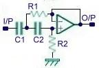
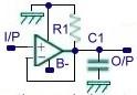
3. Voltage follower buffer amplifier circuit:
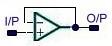
The potential of the O/P output is the same as the potential of the I/P input
Both single and dual power supplies can work
4. Comparator comparator circuit:
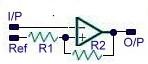
O/P output is Logic low when I/P voltage is higher than Ref
O/P output is Logic high when I/P voltage is lower than Ref
R2 = 100 * R1 is used to eliminate the Hysteresis state, which is to strengthen the O/P output, Logic high and low potential difference to improve the sensitivity of the comparator. (R1=10 K, R2=1 M)
Both single and dual power supplies can work
5. Square-wave oscillator Square wave oscillation circuit:
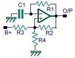
R2 = R3 = R4 = 100 K
R1 = 100 K, C1 = 0.01 uF
Freq = 1 /(2Ï€* R1 * C1)
6. Pulse generator pulse generator circuit:
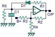
R2 = R3 = R4 = 100 K
R1 = 30 K, C1 = 0.01 uF, R5 = 150 K
O/P output On Cycle = 1 /(2Ï€* R5 * C1)
O/P output Off Cycle =1 /(2Ï€* R1 * C1)
7. Active low-pass filter Active low-pass filter circuit:
R1 = R2 = 16 K
R3 = R4 = 100 K
C1 = C2 = 0.01 uF
Magnification Av = R4 / (R3+R4)
Freq = 1 KHz
8. Active band-pass filter Active bandpass filter circuit:
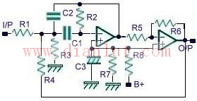
R7 = R8 = 100 K, C3 = 10 uF
R1 = R2 = 390 K, C1 = C2 = 0.01 uF
R3 = 620, R4 = 620K
Freq = 1 KHz, Q=25
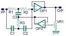
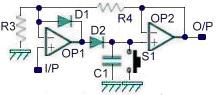
9. Window detector window detector circuit:
When the I/P potential is higher than the OP1+ terminal potential, Led 1 dark/Led 2 is bright
When the I/P potential is higher than the OP2-terminal potential, Led 1 is bright/Led 2 dark
Only when the I/P potential is higher than the OP2-terminal potential but lower than the OP1+ terminal potential, both Led 1 and Led 2 are bright at the same time.
If the R1, R2, and R3 values ​​are properly selected, it can be used to check if the I/P potential is within specifications.
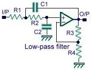
10. Low-pass filter low pass filter circuit:
R1 = R2 = 24 K
C1 = 2 * C2 = 940 pF, C2 = 470 pF
6 dB High-cut Freq = 10 KHz
11. High-pass filter high-pass filter circuit:
C1 = 2*C2 = 0.02 uF, C2 = 0.01 uF
R1 = R2 = 110 K
6 dB Low-cut Freq = 100 Hz
12. Adj. Q-notch filter Bandwidth tunable filter circuit:
R1 = R2 = 2 * R3
C1 = C2 = C3 / 2
Freq = 1 /(2Ï€* R1 * C1)
VR1 adjusts the negative feedback, and the larger the Q, the lower the Q value. (This indicates that the frequency band is widened, but the attenuation value is relatively reduced.)
R1, R2, R3, C1, C2, and C3 are Twin-T filter structures.
13. Wien-bridge Sine-wave Oscillator bridge sine wave oscillation circuit:
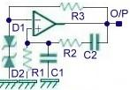
R1 = R2, C1 = C2
R3 and D1, D2 Zener generates fixed-point negative feedback
Freq = 1 / (2Ï€* R1 * C1)
D1 and D2 can use the Lamp effect better (generating impedance negative coefficient of variation)
14. Peak detector peak detector circuit: (examples are positive peak detection)
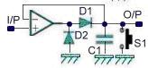
This circuit only provides a reference for thinking (the right circuit has a magnification function)
Eo = Ei * (R4 + R3) / R3
S1 is a continuous sampling switch that responds to changing peaks.
15. Positive-peak detector positive peak detector circuit:
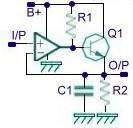
R1 = 1 K, R2 = 1 M, C1 = 10 uF
Only when the I/P potential is higher than the OP-terminal potential can Q1 be turned on and the O/P potential continues to rise.
The positive peak must be lower than the positive value of the power supply and the resulting data is the highest value.
16. Negative-peak detector negative peak detector circuit:
R1= 1 M, C1= 10 uF
The O/P potential continues to decrease only when the I/P potential is lower than the OP-terminal potential.
The negative peak must be higher than the negative value of the power supply and the resulting data is the highest value.
17. RMS (Absolute value) detector absolute value detector circuit:
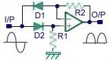
Regardless of the polarity of the I/P terminal, it can be output by the O/P terminal. If the back end is connected to the positive peak detector circuit, the RMS value can be obtained.
Incremental encoders provide speed, direction and relative position feedback by generating a stream of binary pulses proportional to the rotation of a motor or driven shaft. Lander offers both optical and magnetic incremental encoders in 4 mounting options: shafted with coupling, hollow-shaft, hub-shaft or bearingless. Single channel incremental encoders can measure speed which dual channel or quadrature encoders (AB) can interpret direction based on the phase relationship between the 2 channels. Indexed quadrature encoders (ABZ) are also available for homing location are startup.
Incremental Encoder,6Mm Solid Shaft Encoder,Hollow Rotary Encoder,Elevator Door Encoder
Jilin Lander Intelligent Technology Co., Ltd , https://www.jilinlandertech.com