MOS tube introduction
When designing a switching power supply or a motor driving circuit using a MOS tube, it is generally necessary to consider factors such as the on-resistance of the MOS, the maximum voltage, the maximum current, and the like.
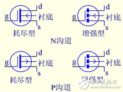
MOS tube conduction characteristics
Turn-on means as a switch, which is equivalent to a switch closure.
The characteristics of the NMOS, Vgs is greater than a certain value will be turned on, suitable for the case when the source is grounded (low-side drive), as long as the gate voltage reaches a certain voltage (such as 4V or 10V, other voltage, see the manual) It is.
The characteristics of the PMOS, Vgs is less than a certain value will be turned on, suitable for the case when the source is connected to VCC (high-end drive). However, although PMOS can be conveniently used as a high-side driver, NMOS is usually used in high-end driving because of high on-resistance, high price, and low replacement.
MOS switch tube loss
Regardless of whether it is an NMOS or a PMOS, there is an on-resistance after the conduction. Therefore, while the current flows between the DSs, there is a voltage at both ends, so that the current consumes energy on the resistor, and the energy consumed is called Conduction loss. Selecting a MOS transistor with a small on-resistance reduces the conduction loss. The current low-power MOS tube on-resistance is generally in the order of a few milliohms, tens of milliohms
When MOS is turned on and off, it must not be completed in an instant. The voltage across the MOS has a falling process, and the current flowing through has a rising process. During this time, the loss of the MOS tube is the product of voltage and current, called switching loss. Usually, the switching loss is much larger than the conduction loss, and the faster the switching frequency, the large product of the voltage and current at the turn-on instant, and the loss is large. By reducing the switching time, the loss per turn-on can be reduced; reducing the switching frequency can reduce the number of switches per unit time. Both of these methods can reduce switching losses.
MOS tube driver
MOS tube conduction does not require current, as long as the GS voltage is higher than a certain value, it can be. However, we still need speed.
It can be seen in the structure of the MOS transistor that there is a parasitic capacitance between GS and GD, and the driving of the MOS transistor is actually charging and discharging the capacitor. The charging of the capacitor requires a current, because the capacitor can be regarded as a short circuit when charging the capacitor, so the instantaneous current will be relatively large. The first thing to note when selecting/designing a MOS tube driver is the amount of transient short-circuit current available.
Mosfet parameter meaning Description: Vds: DS breakdown voltage. When Vgs=0V, the maximum voltage that MOS DS can withstand Rds(on): DS's on-resistance. When Vgs=10V, MOS DS Resistance Id: Maximum DS current. Vgs will decrease with increasing temperature: Maximum GS voltage. Generally: -20V~+20VIdm: Maximum pulse DS current. It will decrease with increasing temperature, reflecting an impact resistance. Also related to pulse time Pd: Maximum dissipated power Tj: Maximum operating junction temperature, usually 150 degrees and 175 degrees Tstg: Maximum storage temperature Iar: Avalanche current Ear: Repeated avalanche breakdown energy Eas: Single pulse avalanche breakdown Energy BVdss: DS breakdown voltage Idss: saturated DS current, uA level current Igss: GS drive current, nA level current. gfs: transconductance Qg: G total charge quantity Qgs: GS charge quantity Qgd: GD charge quantity Td ( On): On-delay time, from the time when the input voltage rises to 10% until the time when Vds drops to 90% of its amplitude Tr: rise time, the output voltage VDS drops from 90% to the time Td of its amplitude 10% ( Off): turn off the delay time, the input voltage drops to 90% starts at 10% of the time when VDS rises to its turn-off voltage Tf: Fall time, the output voltage VDS rises from 10% to 90% of its amplitude (refer to Figure 4). Ciss: Input capacitance, Ciss=Cgd + Cgs.Coss: Output capacitance, Coss=Cds +Cgd. Crss: Reverse transmission capacitance, Crss=Cgc.
Corner light ,led Corner light ,Waterproof Corner Light,Bright LED corner light
Kindwin Technology (H.K.) Limited , https://www.szktlled.com