With the rapid development of the wireless communication industry, a variety of communication technology standards have been created, such as Bluetooth, GSM, WiFi, ZigBee, etc., and communication frequencies range from hundreds of megahertz to several megahertz. From the perspective of application cost and performance, radio frequency (RF) chips with wide tuning range and high reliability have wide application value, so it is one of the design hotspots of current wireless communication systems. The performance of a voltage-controlled oscillator (VCO), which is the core component of a wireless RF transceiver chip, is directly related to the quality of the RF chip. Therefore, multi-standard communication technology imposes high performance requirements on the VCO: obtaining a wider tuning range and lower phase noise (Nphase). Reference [1] introduced a gain-adjustable CMOS LC VCO with an adjustment range of only 4.39 to 5.26 GHz, a power consumption of 9.7 mW, and a Nphase of -113.7 dBc/Hz at 1 MHz offset. In [2], a CMOS VCO with quadrature coupling structure is designed. The tuning range is only 3.*.9 GHz, the power consumption is 8 mW, and the Nphase is -114 dBc/Hz at 1 MHz offset. In order to solve the above problems of narrow bandwidth and high Nphase value, a 0.35μm SiGe BiCMOS differential LC VCO was designed.
1 LC VCO circuit design1.1 Low Nphase value VCO design
The Nphase value is an important performance indicator of the VCO circuit and is usually defined as the ratio of the noise signal power to the total output power of the output signal at a given frequency. Classic D. is often used in actual analysis. B. Leeson's phase noise L(Δω) equation
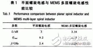
Where: F is the empirical coefficient, different processes have corresponding values; k is the Boltzmann constant; T is the Kelvin temperature; Ps is the signal power; Δω is the deviation frequency, Δω1/f3 is the active in the oscillator The flicker noise angular frequency of the device; ω0 is the angular frequency of the oscillating signal; QL is the quality factor of the LC cavity. Nphase is mainly composed of thermal noise and flicker noise. The flicker noise is related to the symmetry of the VCO signal waveform. The VCO can be improved by designing a signal swing symmetrical VCO to reduce the impact on Nphase. A differential structure allows the output waveform to be completely symmetrical. It is known from equation (1) that the Nphase of the VCO is inversely proportional to the square of the QL. When the quality factor of the LC resonator is increased, the selectivity to the resonant frequency is enhanced, and the spectral curve at the resonance point becomes sharper. This suppresses the influence of the external circuit on the Nphase of the VCO. High-Q on-chip inductors are required to be used whenever possible. On-chip spiral inductors based on microelectromechanical systems (MEMS) technology, because of its new technology such as reducing loss liner, reducing metal coil loss and constructing three-dimensional structure, the inductance performance is better than the traditional on-chip inductor, and the Q value. It is also improved, and it is small in size, low in power consumption, and easy to integrate on-chip.
Table 1 compares the performance of planar spiral inductors with MEMS multi-layer spiral inductors. It can be seen from the table that the MEMS multilayer spiral inductors have higher Q values ​​at lower power frequencies. The inductor was modeled and simulated using the HFSS device software design tool, and the inductance value of the inductor at 4.0 GHz was L≈1.04 nH, Q≈11.3. Modern communication systems require VCOs with higher frequencies, which require higher Nphase values ​​at higher frequencies for VCOs, which are generally higher than the corner frequencies of the VCO, causing thermal noise to become the primary source of Nphase values. The thermal noise in the VCO circuit is mainly related to the tail current. When the tail current increases, the thermal noise will increase, and vice versa. However, reducing the tail current blindly will make the output signal swing too small, and even cause the circuit to work. Stable, so that the vibration is stopped. Therefore, the transconductance of the negative resistance circuit is preferred in the design, so that when the circuit has a sufficiently large amplitude of oscillation, excessive thermal noise is not generated and the Nphase value is increased.
1.2 VCO circuit structure
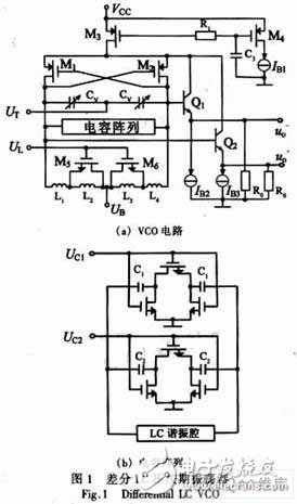
The designed LC VCO circuit topology is shown in Figure 1(a). M1 and M2 are cross-PMOS tube structures, which form a negative resistance link; M3, M4 and IBl form a tail current mirror circuit. In order to reduce the influence of the 1/f noise of the circuit on the L(Δω) of the VCO, PMOS is usually used. The reason is that the PMOS tube has a lower flicker noise corner frequency than the NMOS tube, and the width and length ratio of M3 and M4 are generally larger, which can improve low frequency flicker noise; L1 to L4, CV, M5, M6 and capacitor The falling column constitutes the LC cavity. Figure 1 (b) shows the internal structure of the capacitor switch array, where C1 and C2 are capacitor arrays. By switching to achieve multi-band VCO, the method uses three NMOS transistors to control the opening or closing of the capacitor. When UC1, 2 is high, the NMOS is in the on state, and the capacitor array is in the on state, instead UC1, 2 is low. At the level, the capacitor array is in the off state, thus achieving multi-band switching; in addition to the capacitor array, the switching is designed to achieve a wider range of band switching, and two NMOS transistors M5 and M6 are used for the inductor. Switching, when UL gives the closing signal, M5, M6 is equivalent to short circuit, the inductance at this time is L1 or L4, when UL gives the open signal, M5, M6 is equivalent to open circuit, the inductance at this time is equivalent L1 and L2 or the sum of L3 and L4; CV is a cumulative MOS capacitor, which has a larger tuning range and better monotonicity than a common varactor, and the tuning voltage of the MOS capacitor is 0-3.3 V in the design. The capacitance varies from 0.7 to 1.4 pF. Q1, Q2 and constant current sources IB2, IB3 form an output buffer for the purpose of amplifying the signal. In addition, in Figure 1(a), Q1 and Q2 are BJT, and all others are CMOS devices. By using SiGe BiCMOS technology, the operating speed and driving capability of the buffer are improved, and the VCO oscillation waveform buffer output is reduced. The external circuit interferes with the noise of the VCO oscillation.
Game Machine,machine games,coin operated games,slot games
Guangzhou Ruihong Electronic Technology CO.,Ltd , https://www.callegame.com