This paper describes an image remote collection terminal based on STM32F407, which is discussed from two aspects: terminal acquisition hardware design and terminal acquisition software design. The validity and rationality of the acquisition terminal are verified by experiments.
1, terminal acquisition hardware designThe main block diagram of the system is shown in Figure 1. It is mainly composed of several important parts such as STM32F407 chip, OV7670CMOS image sensor and PC software. STM32F407 is the core of the entire remote acquisition terminal, which plays a key role in the connection. On the one hand, it will complete the acquisition and preprocessing of the underlying signals. On the other hand, it will transmit the collected color image data to the host computer through the network in real time. The contents of these two sections will be highlighted.
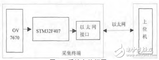
Figure 1 System main block diagram
1.1, STM32F407 and OV7670 hardware connectionIn FIG. 2, the 8-bit image data output by the OV7670 via the DCMI interface is received by the PH9-PH12, PH14, PI4, PI6, and PI7 interfaces of the STM32F407. The SIO_C and SIO_D interfaces of the OV7670 are connected to the STM32F407PF8 and PF9 pins respectively, and the initial configuration of the camera is realized through this interface. The OV7670CMOS camera is configured with COM7 register to collect 16-bit image data of RGB565, and the data is transmitted to the image data buffer through DMA. When the vertical synchronization interrupt arrives, it indicates that one frame of image data is filled in the buffer, and the controller takes out the image. The data buffered by the data is processed for subsequent processing and then transmitted to the host computer. The connection diagram of the camera and STM32F407 is shown in Figure 2:
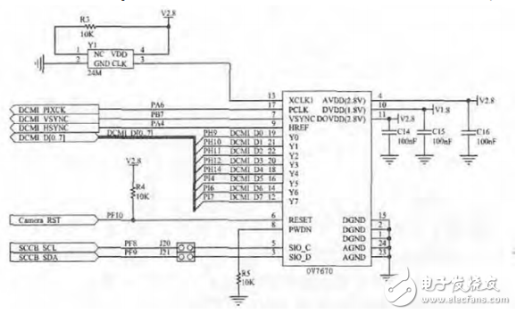
Figure 2 OV7670 and STM32F407 connection circuit diagram
1.2, STM32F407 Ethernet communication interface circuitThe Ethernet communication interface module is composed of the Ethernet MAC built in the CPU, the dedicated 10/100M PHYLAN8720A, HR11105A, and RJ45 network port. The Ethernet physical layer device LAN8720A acts as a physical layer device for the TCP/IP protocol. The HR911105A is an RJ45 network interface device. When the host PC has data requirements, the data request command first enters the controller through the twisted pair, HR911105A and STM32F407 Ethernet modules, and the command data is internally converted to the SPI format, and then sent to the STM32F407 through the SPI bus. The conversion of SPI format data to Ethernet data is implemented in STM32F407. After the IP encapsulation is completed, the data is transmitted to the host computer through the Ethernet module of the STM32F407, the LAN8720A and HR911105A interfaces, and the twisted pair. The chip pin connection diagram is shown in Figure 3.
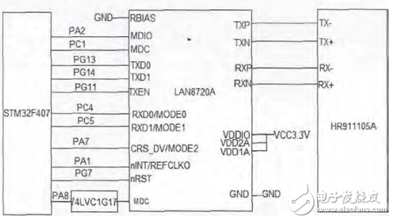
Figure 3 LAN8720A and STM32F407 hardware connection circuit diagram
2, terminal acquisition software designThe software design mainly includes implementing TCP/IP protocol on STM32F407 and communicating with the host computer to control the acquisition and transmission of image data by OV7670CMOS image sensor. STM32F407 program design is implemented in KeiluVision4 environment, which mainly includes the following two parts: one is the acquisition of analog signal by OV7670; the other is the realization of remote transmission data. This article mainly introduces the implementation method of STM32F407 program.
2.1, OV7670 completes the acquisition of analog signalsIn the design of image acquisition software, the initialization of each part of the system is the most crucial step. Only after the initialization of each part is successful, the image acquisition function can be realized. The image acquisition initialization program mainly includes initialization of the system clock, SCCB interface, DMA, DCMI interface, OV7670 camera, and the like. After the system initialization setting is successful, the microcontroller continuously monitors the VSYNC signal level change and controls the reading of the data according to the interrupt condition generated by VSYNC. The terminal image acquisition program flow chart is shown in Figure 4:
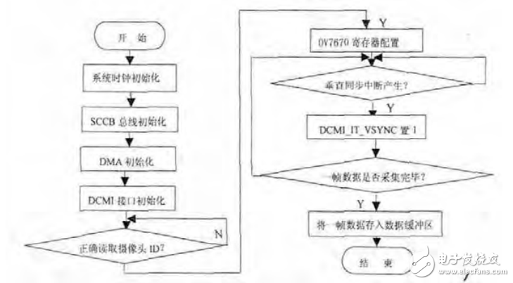
Figure 4 image acquisition program flow chart
(1) Set the relevant parameters of SCCB
Since the configuration of the camera working parameters is mainly realized by SCCB, when the system is designed for software, the SCCB related program is first designed, and then the relevant parameters of the camera are set by the SCCB. The important functions of the SCCB design are as follows.
Voidsccb_bus_init(void)
{
GPIO_InitTypeDefGPIO_InitStructure; / / structure initialization
RCC_AHB1PeriphClockCmd(RCC_AHB1Periph_GPIOF, ENABLE);//Enable GPIOF clock
GPIO_InitStructure. GPIO_Pin=GPIO_Pin_8|GPIO_Pin_9;//SCCB_SIC: PE2, SCCB_SID: PE3
GPIO_InitStructure. GPIO_Mode=GPIO_Mode_OUT;//set to output
GPIO_InitStructure. GPIO_OType=GPIO_OType_PP; / / set to push mode
GPIO_InitStructure. GPIO_PuPd=GPIO_PuPd_UP;//suspension mode
GPIO_InitStructure. GPIO_Speed=GPIO_Speed_50MHz; //50MHz clock frequency
GPIO_Init(GPIOF,&GPIO_InitStructure);}
(2) OV7670 register configuration
After completing the SCCB initialization, start and stop and other related procedures, configure the OV7670 register to complete the setting of the operating parameters, including display mode, output format, gain control, and so on. The register configuration of the OV7670 is as follows:
Constuint8_tOV7670_reg[OV7670_REG_NUM][2]={
{0x12, 0x14}; / / set to VGA display mode
{0x40,0xd0};//RGB565 output format
{0x3e, 0x00}; / / PCLK does not divide
{0x71, 0x00}; / / non-test mode
/*Image resolution configuration*/
{0x32, 0x80},
{0x17, 0x16},
{0x18, 0x04},
{0x19,0x02},
{0x1a, 0x7a},
{0x03, 0x03},. . . . . . }
External Axial Fan,External Rotor Fan,External Rotor Axial Fan,Axial Cooling Fan
Hangzhou Jinjiu Electric Appliance Co Ltd. , https://www.jinjiufanmotor.com