Aiming at the problems of large size and high price of existing 3D imaging equipment, a micro-embedded 3D image sensor is designed by using FPGA high-speed parallel processing capability and image sensor. Through the FPGA synchronization setting, the image data of the dual CMOS image sensor is acquired, transferred to the SDRAM for buffering, and the pixels are combined by the line pixels, and the left and right stereo pair images are stored.
The naked-eye 3D technology is the key development area pointed out in the “13th Five-Year National Strategic Emerging Industry Development Planâ€. The plan shows the core technology innovations such as accelerating virtual reality, augmented reality, holographic imaging, and naked-eye 3D graphics display (naked eye 3D). The determination to develop [1]. The 3D camera of film and television shooting is bulky, complicated in structure and expensive, and is not suitable for the application of embedded systems, which seriously restricts the industrial application of naked eye 3D technology. The CPU of portable products and TV sets does not have the interface and capability for synchronously acquiring 3D images. Therefore, image 3D sensors can only use FPGA or CPLD devices to process image data in parallel at high speed [2].
In this paper, an embedded miniature 3D image sensor is designed according to the principle of human eye bionics. The hardware logic method is studied to realize the acquisition, transmission, storage and display of 3D images. It provides a means for obtaining 3D image data for the portable field, and strives to solve the naked eye 3D. Technical bottlenecks faced by technology productization.
01 system design ideas
According to the principle of stereo vision, 3D images should be acquired synchronously and meet the requirements of imaging sharpness, optical axis convergence, and parallax matching.
The 3D image sensor system structure includes two CMOS image sensors and SDRAM for buffering image data. In order to synchronously configure and acquire the two image sensors, only FPGA (or CPLD) can be selected as the logic control chip.
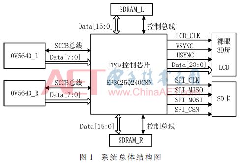
The overall structure of the system is shown in Figure 1, using FPGA + dual CMOS + dual SDRAM hardware structure. The FPGA selects EP3C25Q240C8N of Altera Company as the main control chip; in order to meet the requirements of image sensor resolution, CMOS image sensor adopts OV5640 with 5 megapixels; FPGA collects and buffers the image data acquired by OV5640 to SDRAM, and its capacity should satisfy one frame. Storage requirements for high definition image data. The guiding idea of ​​the image capturing and video recording method of the 3D image sensor is to combine the image data of two OV5640s acquired synchronously in line pixels, and store the image in the full-width or half-width stereo pair in the left and right format to the SD card. Using the naked-eye 3D LCD screen as a real-time monitoring device, the FPGA logic controls the pixel reconfiguration of the left and right images, and then inputs it to the naked eye 3D display.
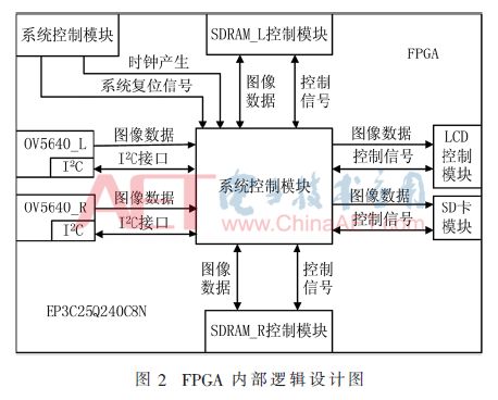
Since the FPGA is not a CPU structure, but a customizable device that implements complex logic, it is necessary to design a logic control block for the connected device. According to the functional requirements of the 3D image sensor, according to the flow of image data, the internal logic design of the FPGA should include an image acquisition module, an SDRAM cache control module, an SD card storage module, a naked-eye 3D LCD display control module, and a system control module.
The OV5640 operates at 24 MHz, the FPGA external clock is 50 MHz, the SDRAM operating clock is 100 MHz, and the LCD's operating clock is 25 MHz. Therefore, the system control module needs to solve the problem of data communication across the clock domain. The internal logic design of the FPGA is shown in Figure 2.
02 image data acquisition and caching method
In 3D shooting, if the two image sensors are not effectively synchronized, there will be a time difference in the exposure imaging of the moving object, with the result that the left and right eye images are not synchronized, so that the 3D vision cannot be formed and the display fails. Therefore, the 3D image sensor must ensure pixel-level synchronization, and use the hardware logic control of the FPGA to complete accurate synchronization configuration and synchronous acquisition of the image sensor.
2.1 Image sensor synchronization configuration and data acquisition
The working register of the OV5640 is configured by SCCB (serial camera control bus) [3]. The image output data of the image sensor is set to RGB565, and according to the resolution of the image monitoring device, 1 024×768 and 800×600, The resolution of the left and right eye image sensors is set to 512×768 and 400×600 according to the half-width principle, and the frame rate is 30 f/s, to verify whether the logic algorithm of the FPGA is correct.
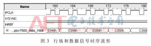
After the initialization of the OV5640 is completed, the image sensor starts to work, and the image data is output from the data interface according to the set frame rate. The FPGA starts to acquire the image data Data[7..0] of the OV5640 under the control of PCLK (pixel clock), HREF (row sync signal) and VSYNC (field sync signal), and the design logic algorithm will collect the adjacent two The byte data is converted into 16-bit image data. Using Signal-tapII to collect the timing waveform of the line signal and data signal online, as shown in Figure 3, when the PCLK is at the rising edge, the field signal is detected. When VSYNC is at a low level and HREF is at a high level, the image data is being collected. When the VSYNC signal goes from low level to high level, it means to start collecting a new frame of image data. Looking at the waveform of Figure 3, the logic algorithm for data acquisition of the designed image sensor is correct.
2.2 Image Data Cache
In order to solve the problem of data communication across clock domains, the FPGA internally built wr_FIFO and rd_FIFO to connect OV5640 and SDRAM, wr_FIFO is used to receive image data acquired by OV5640, and rd_FIFO is used to buffer image data output to LCD. When wr_FIFO receives wr_req (write data request), the data collected by OV5640 is buffered into wr_FIFO; when rd_FIFO receives rd_req (read data request), rd_FIFO outputs the buffered data to LCD display.
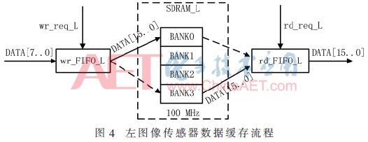
Due to the large amount of 3D video image data, high transmission speed and pixel level synchronization, in order to ensure the effective processing of data, the SDRAM control module is designed, and the SDRAM is used for time-sharing operation [4]. When the SDRAM performs a write operation, the data is first written to BANK0, and after one frame of image data is written, it is switched to BANK3; when the SDRAM performs a read operation, the same logic is used to switch BANK. According to the above logic, the wheel sequential operation SDRAM algorithm is packaged into an SDRAM controller, so that the buffering of image data in the SDRAM is more simplified and efficient. The data buffer operation flow of the left image sensor is shown in FIG. 4 .
03 image storage
SD card has the advantages of small size, low power consumption, fast reading speed, etc., so it is widely used in portable storage [5]. SPI works in master-slave mode. The system uses SPI mode to communicate between SD card and FPGA. It is composed of SPI_CLK (clock signal), SPI_MISO (master input slave output), SPI_MOSI (master output slave input), SPI_CSN (chip select signal). composition.
The left and right stereo image with resolution of 2 048×768 is stored in the SD card in BMP format, which is divided into three processes: stereo image data is converted into BMP image data format; SD card initialization; SD card write operation control [6] . The image data collected by the 3D image sensor is RGB565, and the SD card is stored in the true color RGB888 format. Therefore, RGB565 to RGB888 operation is required. There are two options: one is to adopt the low-order zero-padding method, and the other is to RGB565 data to the high-displacement bit. After the low level of the original low data, the system has carried out experiments on both programs, and the viewing effect is consistent. The initialization of the SD card is implemented in accordance with the initialization process of the SD card. The FAT16 file system is used to perform sector management on the SD card for stereo image to be correctly written. The Verilog_HDL (Hardware Description Language) is used to write the FAT table, the root directory and the BMP file information of 54 B to the physical address corresponding to the SD card. . Under the control of the left and right data channels, the left and right image data are written into the data area of ​​the SD card, and the left data channel strobe timing diagram is as shown in FIG. 5, and the right data channel strobe timing relationship is the same.

04 image display
The collected image is displayed by using an 8-inch open-hole 3D display. The naked-eye 3D display is compatible with 2D and 3D display, so two logical algorithms of left and right stereo pair display and 3D display after pixel reconfiguration are respectively designed. The driving mode of the LCD is DE mode, the DE signal is equivalent to the composite signal of the two sync signals in the field, and the two counters of DE_h and DE_v are controlled by two counters h_cnt and v_cnt, the logic is DE=DE_h&DE_v, when DE is high At the level, the LCD displays the received image data.
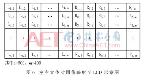
In the 2D display, the left and right stereo pair images with certain parallax are mapped to the LCD, and the left and right data strobe signals are switched according to the timing standard, so that the left and right image data are transmitted to the LCD for display. The VGA interface and the LCD interface are designed on the hardware, and the stereo pair image is mapped to the LCD TV and the LCD respectively. The mapping principle is the same, but the timing is different. The schematic diagram of the left and right stereo image mapping to the LCD is shown in FIG. 6 .
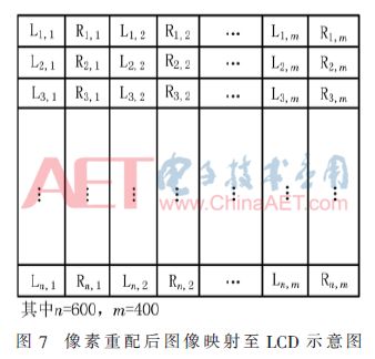
In 3D display, the left and right image data are respectively mapped to the left-eye and right-eye sub-screens [7] of the naked-eye 3D display, that is, the left image data is mapped on the odd-column pixels of the screen, and the right image data is mapped on the even-pixel pixels of the screen. On the top, the left and right image data are subjected to line compression logic design, and are alternately written into the LCD according to the clock frequency to complete pixel reconfiguration. The naked-eye 3D display is structurally different from the ordinary 2D display, and there are also differences in viewing angles. When the human eye is in the independent viewport, the left and right eyes can independently see the images on the left and right sub-screens, and form the naked eye 3D effect through the brain visual center fusion [8]. When the human eye is in a non-independent viewing zone, the left and right eyes can respectively see the images on the left and right sub-screens, and a ghost image is formed at this time to affect the viewing effect. A schematic diagram of mapping left and right stereo pairs of image pixels to the LCD is shown in FIG.
05 simulation analysis and experiment
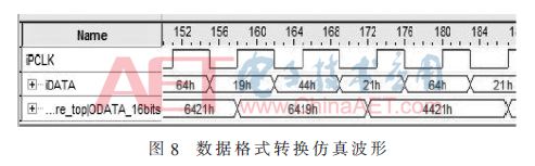
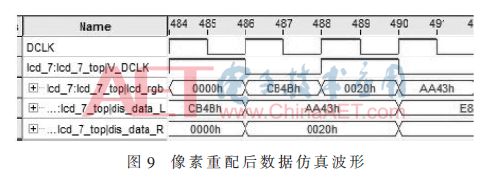
The OV5640 captures 8 bit of image data and converts it to 16 bit data in RGB565 format during the SDRAM buffer process. The embedded logic analyzer Signal-tapII is used to simulate the conversion. The simulation waveform is shown in Figure 8. The value verifies that the logic is designed correctly. The image data displayed on the naked eye 3D screen after pixel reconfiguration is simulated and analyzed. The waveform is as shown in FIG. 9. The online simulation shows that the image data in the 3D display and the image data acquired by the left and right image sensors are strictly consistent.
The system uses an LCD TV and a naked-eye 3D display to perform an experiment, and accurately and stably input and display the captured high-definition stereo image. The 3D image sensor re-matches the stereoscopic image pixels and inputs them to the naked eye 3D display, which is effective. The experimental results show that the designed 3D image sensor and its logic algorithm can complete the acquisition, transmission, storage and display of 3D images, and verify the correctness of the system hardware logic algorithm.
06 conclusion
The portable 3D shooting device has broad development prospects. The 3D image sensor designed according to the stereoscopic vision bionic principle of the human eye utilizes the advantages of FPGA high-speed parallel processing, which makes the hardware architecture more integrated and solves the 3D video image source, storage and pixel. Re-allocation and other issues. The system works stably and has good portability. It can support different image sensors and displays by modifying the module program, and supports 2D and 3D display, which has good compatibility.
The 3D image sensor provides a means of 3D image acquisition, and the user can record the 3D scene anytime and anywhere, and can reproduce the three-dimensional scene on the naked-eye 3D device to obtain a sense of presence and immersion. The development of 3D image sensor provides a useful reference for the design of ASICs for 3D image sensors.
Anyang Kayo Amorphous Technology Co.,Ltd is located on the ancient city-Anyang. It was founded in 2011 that specializes in producing the magnetic ring of amorphous nanocrystalline and pays attention to scientific research highly,matches manufacture correspondingly and sets the design,development,production and sale in a body.Our major product is the magnetic ring of amorphous nanocrystalline and current transformer which is applied to the communication, home appliances, electric power, automobile and new energy extensively. We are highly praised by our customers for our good quality,high efficiency,excellent scheme,low cost and perfect sale service.
Nano-crystalline Common Mode Choke Cores have high saturation magnetic induction that can reduce the volume of CMC,outstanding ability to resist unblanced current, excellent impedance and tamperature stability.So it can be used to the inverter circuit ,frequency converter.UPS, switching power,EMC filter and new energy.
Nano Cmc Iron Core,Best Cmc Core,New Energy Cmc Core,Utility Cmc Core,Real Cmc Core
Anyang Kayo Amorphous Technology Co.,Ltd. , https://www.kayoamotech.com