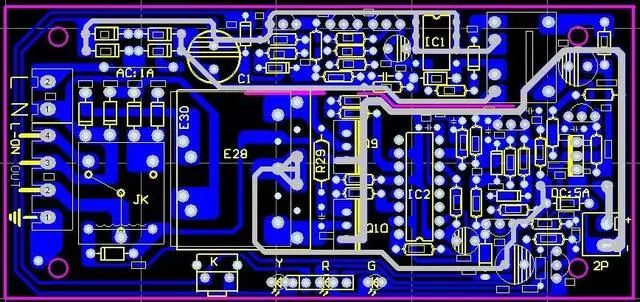
A: This board's PCB design requirements are not high, use finer lines, automatically cloth it
Comments: Automatic routing will inevitably take up a larger PCB area, and at the same time produce many times more than the manual wiring multiple vias, in a large batch of products, PCB manufacturers price reduction factors in addition to business factors, is the line width and The number of holes affects the yield of the PCB and the number of bits consumed, saves the cost of the supplier, and provides a reason for the price reduction.
Two: These bus signals are pulled with resistors, feeling more at ease.
Comments: There are many reasons why signals need to be pulled down, but not all of them need to be pulled. The pull-up resistor pulls a simple input signal, the current is also less than tens of microamperes, but pulling a driven signal, the current will reach the milliampere level, the current system is often the address data of each 32-bit, there may be After 244/245 isolated buses and other signals are pulled up, several watts of power are consumed by these resistors.

Three: How to deal with these unused I/O ports of CPU and FPGA? Let it be empty first, and later say.
Comments: If the unused I/O port is left unconnected, a little interference from the outside world can become an input signal for repeated oscillations. The power consumption of the MOS device basically depends on the number of flipping of the gate circuit. If it is pulled up, there will be micro-ampere current per pin, so the best way is to set it to output (of course, it can't be connected to other drivers).

Four: This FPGA has so many things left to use, you can make full use of it
Comments: The power consumption of FGPA is proportional to the number of flip-flops used and their number of flips, so the power consumption of FPGAs of the same model at different times in different circuits may differ by a factor of 100. Minimizing the number of flip-flops that are flipped at high speed is a fundamental way to reduce FPGA power consumption.
Five: The power consumption of these small chips is very low, do not have to consider
Comments: For the internal less complex chip power is very difficult to determine, it is mainly determined by the current on the pin, an ABT16244, no load, then power consumption is probably less than 1 mA, but its indicator is each foot Can drive 60 mA load (such as matching tens of ohms resistance), that is, full-load power consumption up to 60 * 16 = 960mA, of course, only the power supply current is so large, the heat falls on the load body.
Six: The memory has so many control signals, I only need to use the OE and WE signals on this board. The chip selects the ground, so the data comes out much faster when reading.
Comments: Most memory power consumption when the chip select is valid (regardless of OE and WE how) will be more than 100 times more than when the chip select is invalid, so should use CS as far as possible to control the chip, and meet the other requirements It is possible to shorten the width of the chip select pulse.
Seven: How do these signals overshoot? As long as they match well, they can be eliminated.
Comments: In addition to a few specific signals (such as 100BASE-T, CML), there are overshoots, as long as it is not very large, it does not always need to be matched, even if the match is not to match the best. The output impedance like TTL is less than 50 ohms, and some are even 20 ohms. If such a large matching resistor is used, the current is very large, power consumption is unacceptable, and the signal amplitude is too small to be used. Furthermore, the output impedance of the general signal at the output high level and the output low level is not the same, and there is no way to achieve an exact match. Therefore, the matching of signals such as TTL, LVDS, and 422 can be accepted only by overshoot.
Eight: The reduction of power consumption is a matter for hardware personnel, and it does not matter with software.
Comments: The hardware is just taking a stage, but the software is singing. Almost every chip on the bus is accessed and every signal is flipped by software. If the software can reduce the number of external memory accesses (use more register variables, Using internal CACHE etc., responding to interrupts in time (interrupts are often active low and with pull-up resistors) and other specific measures that compete for specific boards will make a big contribution to reducing power consumption.
Nine: CPU with a larger CACHE, it should be faster
Comments: The increase in CACHE does not necessarily lead to an increase in system performance. In some cases, closing CACHE is faster than using CACHE. The reason is that the data moved to CACHE must be reused multiple times to improve system efficiency. Therefore, in the communication system, only the instruction CACHE is generally opened, and even if the data CACHE is opened, it is limited to a part of storage space, such as a stack portion. At the same time, it also requires that the program design should take into account CACHE's capacity and block size. This involves the length of the key code loop body and the jump range. If a loop is just a little bit bigger than the CACHE, and it is repeated, it will be tragic.
Ten: The memory interface timing is the factory default configuration, without modification
Comments: The default values ​​set by the BSP for the memory interface are set according to the most conservative parameters. In practical applications, reasonable allocation should be made in combination with parameters such as bus operating frequency and waiting period. Sometimes the frequency can be reduced to improve the efficiency, such as RAM access cycle is 70ns, the bus frequency is 40M, set up 3 cycles of access time, that is, 75ns; if the bus frequency is 50M, must be set to 4 In the cycle, the actual access time was slowed down to 80ns.
Eleven: This CPU has a DMA module, use it to move data surely fast
Comments: The real DMA is to start the two devices at the same time after the hardware seize the bus, read it in one cycle, write it there. However, many DMAs embedded in the CPU are just simulations. Before starting each DMA, you must do a lot of preparations (set the starting address and length, etc.). When you transfer, you often read the chip temporarily and then write it out. In other words, moving the data once takes two clock cycles, which is faster than software (no need to fetch instructions, no extra work such as loop jump), but if you only move a few bytes at a time, you need to do a bunch of preparations. It also involves function calls, which is not efficient. So this kind of DMA only applies to big data blocks.
Twelve: The 100M data bus should be considered as a high-frequency signal. As for the frequency of this clock signal, it is only 8K. This is not a problem.
Comments: The value of the data bus is generally sampled from an edge of the control signal or clock signal. As long as sufficient setup and hold times are maintained for this edge, no interference outside of this range will occur. How much influence (of course overshooting should not exceed the maximum voltage value that the chip can withstand), but the clock signal no matter how low the frequency (in fact the spectrum range is very wide), its edge is the key, must guarantee its monotony Sex, and the transition time must be within a certain range.
Thirteen: Since it is a digital signal, the edge is of course the steeper the better
Comments: The steeper the edge, the wider the spectrum range, the higher the energy in the high-frequency part; the higher the frequency of the signal, the easier it is to radiate (eg microwave radio can be made into a mobile phone, and long-wave radio can not be done in many countries). Therefore, the easier it is to interfere with other signals, and the worse the transmission quality on the wire becomes, so the low speed chip can be used as low as possible.
XIV: Signal matching is really troublesome. How can we match it well?
Comment: The general principle is that when the signal transmission time on the wire exceeds its transition time, the signal reflection problem becomes important. The cause of the signal reflection is caused by the uneven line impedance. The purpose of the matching is to make the impedances of the driving end, the load end, and the transmission line close to each other, but the matching is good, and the topology of the signal line on the PCB also has It is very important that a branch on a transmission line, a via, a corner, a connector, and a change in the distance between different positions and ground lines will change the impedance, and these factors will make the reflection waveform extremely complex. Difficult to match, so high-speed signals only use point-to-point methods, reducing vias and corners as much as possible.
MT8-IP67 Waterproof Micro Switch
Features
â—† Designed For Water and Dust Tight(IP67)
â—† Small Compact Sizeâ—† UL&ENEC&CQC Safety Approvals
â—† Long life & high reliability
â—† Variety of Levers
â—† Wide Range of wiring Terminals
â—† Wide used in Automotive Electronics,Appliance and Industrial Control etc.
â—† Customized Designs
Micro Switch Ip67,Microswitch Ip67,Ip67 Waterproof Micro Switch,Waterproof Momentary Micro Switch
Ningbo Jialin Electronics Co.,Ltd , https://www.donghai-switch.com