Switched-mode power supply (SMPS) is a very efficient power converter. Its theoretical value is close to 100%, and it has a wide range of types. According to the topology structure, there are Boost, Buck, Boost-Buck, and Charge-pump. According to the switch control mode, there are PWM and PFM. According to the switch type, there are BJT, FET and IGBT. This discussion focuses on the PWM control Buck and Boost types commonly used for data card power management.
The main components of the switching power supply include: input source, switch tube, energy storage inductor, control circuit, diode, load, and output capacitor. At present, most semiconductor manufacturers integrate switch tubes, control circuits, and diodes into a power management IC of a CMOS/Bipolar process, which greatly simplifies the external circuit. The energy storage inductor is a key device of the switching power supply and plays an important role in the performance of the power supply. At the same time, it is also a product design engineer's focus and debugging object. With consumer electronics devices such as cell phones, PMPs, and data cards, the size of these devices is moving toward light, thin, compact, and fashionable, and this is in line with the greater capacity and larger size of product performance. Inconsistent inductance and capacitance. Therefore, how to reduce the size of the switching power supply inductance (PCB area and height occupied) is an important proposition to be discussed in the context of ensuring product performance. Designers will have to compromise between circuit performance and inductance parameters. (Tradeoff).
Everything has two sides, switching power is no exception. Bad PCB layout design will not only reduce the performance of the switching power supply, but will also strengthen EMC, EMI, grounding and so on. The problems that should be paid attention to and the principles to follow when placing and routing the switching power supply are also another important proposition to be discussed in this paper.
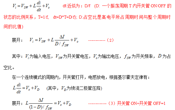
First, the switching power supply duty cycle D, inductance L, efficiency η formula derived
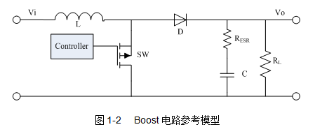
The Buck and Boost switching power supplies have different topologies. This article uses the circuit reference model shown in Figure 1-1 and Figure 1-2.
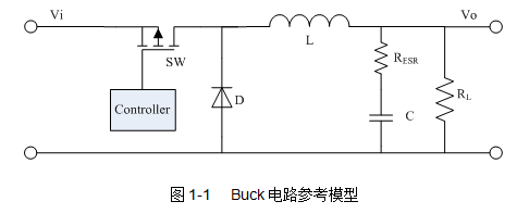
The DCR (Direct Constant Resistance) of the default inductor of the reference circuit model is zero.
Buck/Boost switching power supply, along with the switch on and off, the current waveform of the energy storage inductor shown in Figure 1-3:
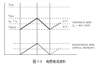
From the figure, it can be seen that the current waveform of the inductor is equivalent to superimposing an AC with a IP-P value of ΔI on the DC IDC. Therefore, the IDC becomes the output current IO and is mainly consumed in the load; the AC ΔI is consumed in the ESR (Equation Serial Resistance) of the load capacitance and becomes the output ripple Vripple.
In a continuous-mode cycle, the switch is closed, charging the inductor, according to Kirchhoff's law:
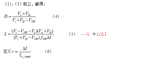
r is also called the current ripple ratio, which is the ratio of the ripple current to the rated output current. For a given Buck switching power supply, this value is generally constant. From equation (5) we can get: The bigger the inductance, the smaller, so the smaller r is. But this often results in the need for a large inductance to do so, so most of the Buck-type switching power supply choose r value between 0.25~0.5.
At this point, we derived the D, L, Lmin, and η of the Buck switching power supply. It should be reminded that all the above formulas are based on the reference circuit model, ignoring the DCR of the inductor.
From (4), we can see that the duty cycle is only related to Vi, Vo, Vsw, and VD. It is easy to build a circuit to calculate D. This is one of the core circuits of the switching power supply controller, but the application to the switching power supply For our part, we can not care.
From (8), we can see that the efficiency η of the switching power supply is only related to Vi, Vo, Vsw, and VD. In fact Vsw and VD are functions of the switching frequency fsw, so η is also a function of fsw, but it is not guaranteed that the higher fsw is, the higher η is. For a given Buck switching power supply, its fsw is determined, so η is a fixed value, especially after ignoring Vsw and VD. Obviously this is inconsistent with the actual situation, the root cause is that "the reference model assumes that the energy storage inductor is the ideal inductor."
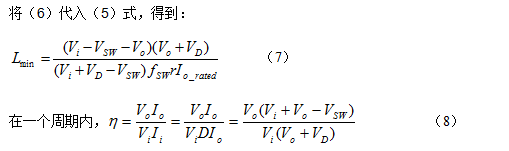
Substituting (5) into (1) yields:
Second, the minimum inductance selection
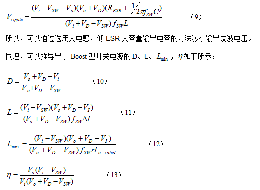
Equations (7) and (12) give the minimum inductance selection formulas for general-purpose Buck and Boost switching power supplies, respectively. For low-power switching power supplies used in consumer electronics such as mobile phones, PMPs, and data cards, Vsw and VD are all between 0.1V and 0.3V, so equations (7) and (12) can be simplified. :
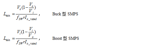
Take the PM power supply MSMC of PM6658 as an example, Vi is 3.8V, Vo is 1.2V, r is 0.3, fsw is 1.6MHZ, Io_rated bit 500mA is Lmin 3.08uH. If the selected inductance tolerance is 20%, 1.25*Lmin=3.85uH. According to the calculated value, the latest standard inductance is 4.7uH, so the minimum inductance recommended by the PM6658 spec is 4.7uH.
Third, the choice of inductance parameters
In addition to the inductance and tolerance described above, the inductor has the following important parameters: Self-resonant frequency (fo), DCR, Saturation current (ISAT), and RMS current (RMS). Current, IRMS). Although there are many parameters, there is only one guideline: try to ensure that the impedance of the inductor under fsw is at a minimum, match the actual circuit with the ideal model, reduce the power consumption and heat of the inductor, and increase the efficiency of the power supply.
3.1 Self-excited frequency fo
In the ideal mode, the inductance has a linear relationship with the frequency and increases with frequency. The actual inductance model is shown in Figure 3-1-1. It is made by connecting the inductor L in series with the RDCR and the parasitic capacitor C. There is a self-excited frequency fo that is inductive when the frequency is less than fo, a capacitance greater than fo, and a maximum impedance in fo. .
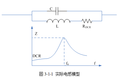
Empirical value: The self-excited frequency fo of the inductor is preferably chosen to be greater than 10 times the switching frequency fsw.
3.2 DC resistance RDCR
The DC resistance RDCR of the inductor itself will consume a part of the power, which will reduce the efficiency of the switching power supply. What's more, this consumption will be carried out through the inductor heating method, which will reduce the inductor's inductance and increase the ripple current and ripple. Voltage, so in terms of switching power supply, according to the DCR typical value or the maximum value provided by the chip data sheet, select the DCR small inductor as much as possible.
3.3 Saturation Current ISAT and Root Mean Square Current IRMS (Inductor Burnout Problem)
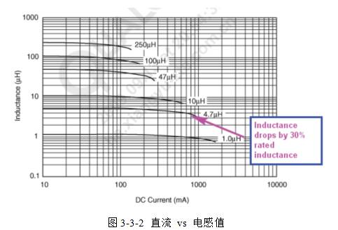
The saturation current ISAT of the inductor refers to the maximum current through which the inductance value drops by 10% to 30% of the nominal value. As shown in Figure 3-3-2, the current at 4.7uH when the inductor drops to 3.3uH is approximately 900mA, so its ISAT (30%) is 900mA.
The rms current of the inductor, IRMS, is the rms current through which the inductor's temperature can rise when it rises from room temperature from 25°C to 65°C.
The size of ISAT and IRMS depends on the order of the magnetic saturation of the inductor and the temperature rise to 65°C.
When the nominal output current is greater than ISAT, the inductor saturates, the inductance value decreases, ripple current and ripple voltage increase, and the efficiency decreases. Therefore, the minimum value of the inductor's ISAT and IRMS should be higher than 1.3 of the rated output current of the switching power supply.
Fourth, the inductor type selection
After the calculation of the minimum inductance value and the selection of the inductance parameters are clarified, it is necessary to make a comparative analysis of some popular types of inductors on the market. The following will be focused on: large inductors and small inductors, wound inductors and stacked inductors, and magnetic shielded inductors Compare with unshielded inductor.
4.1 Large inductance and small inductance in the same size
Here, "same size" means that the physical shape of the inductor is approximately the same, and the "size" index refers to a different capacity. The generally small-capacity inductor has the following advantages:
l Lower DCR, so it will have higher efficiency and less heat at heavy load;
l greater saturation current;
l Faster response to load transients
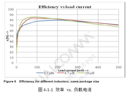
Large-capacity inductors have lower ripple current and ripple voltage, lower AC and conduction losses, and higher efficiency at light loads. Figure 4-1-1 shows the relationship between inductive load current and efficiency for different sizes of Taiyo Yuden's three 2518 packages.
4.2 Wound and Stacked Inductors
Compared to wirewound inductors, stacked inductors have the following advantages:
l Small physical size, taking up less PCB area and height space;
l Lower DCR, higher efficiency in heavy load;
l Low AC loss, higher efficiency at light load;
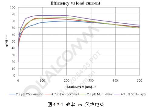
However, the laminated inductor's ISAT is also small, so it will have a large ripple current during heavy load, resulting in a corresponding increase in the output ripple voltage. Figure 4-2-1 shows the relationship between Taiyo Yuden's two wirewound inductors and Samsung's two stacked inductor load currents and efficiency.
4.3 Magnetic Shielding Inductors and Unshielded Inductors
Unshielded inductors have a lower price and smaller size but also generate EMI. Magnetic shielded inductors effectively shield against EMI, making them more suitable for EMI-sensitive applications such as wireless devices, and it also has a lower DCR.
Fifth, inductance selection summary
According to the introduction of the previous sections, we can choose the appropriate inductor according to the following steps:
(1) Calculate Lmin and recommended inductance parameters: fo, DCR, ISAT, IRMS;
(2) Under the premise of ensuring (1), according to the physical size requirements and cost performance, trade-off choices: large inductance or small inductance, laminated inductance or winding inductance, magnetic shielding inductance or non-shielding inductance.
Six, switching power supply layout
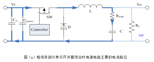
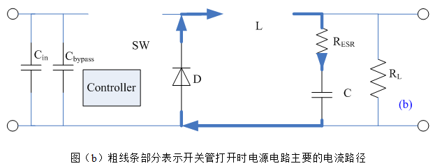
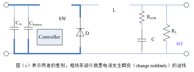
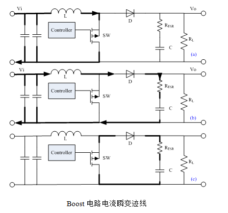
Take the Buck circuit as an example. Regardless of whether the switch is closed-open or open-closed, the transient part of the current is shown in (c). These are the rising or falling edges that produce a very rich harmonic component. . In general, these transient current traces are called AC currents, and the rest are DC currents. Of course, the difference between AC and DC here is not the definition in the traditional textbooks. It means that the PWM frequency of the switch is only a component of the “AC†FFT transform. In the “DCâ€, such harmonic components are very low and can be ignored. . Therefore, it is not surprising that energy storage inductors are “DCâ€. After all, the inductor has the property of preventing transients in the current. Therefore, in the switching power supply layout, the "AC" traces are the most important and need to be carefully considered. This is also the only basic rule that needs to be kept in mind, and applies to other laws and topologies. The following figure shows the Boost circuit current transient trace, paying attention to the difference between it and the Buck circuit.
The 1 inch long, 50mm wide, 1.4mil thick (1 ounce) copper wire has a resistance of 2.5mΩ at room temperature. If a current of 1A flows, the resulting voltage drop is 2.5mV and will not adversely affect most ICs. influences. However, the parasitic inductance of such a 1 inch long wire is 20 nH, and it is known from V=L*dI/dt that if the current changes rapidly, a large voltage drop may occur. The transient current of a typical Buck power supply when the switch is turned on and off is 1.2 times that of the output current, and the transient current generated by off-on is 0.8 times the output current. The conversion time of the FET type switching tube is 30ns and that of the Bipolar type is 75ns. Therefore, when the current of 1A of the switching power supply “AC†part passes through a 1A transient current, a voltage drop of 0.7V is generated. Compared with 2.5mV, 0.7V increases nearly 300 times, so the layout of the high-speed switching part is particularly important.
As close as possible to all the peripheral devices are placed next to the converter, reducing the length of the wiring will be the most ideal layout, but limited to a very limited layout space, the actual often can not be achieved, it is necessary according to the transient The severity of the pressure drop is in the order of priority. For a Buck circuit, the input bypass capacitor must be placed as close to the IC as possible, followed by the input capacitor, and finally the diode. Use a short, thick trace to connect one end to the SW and the other to ground. For the Boost circuit layout, the output bypass capacitors, output capacitors, and diodes are placed in order of priority.
Full Capacity High Speed Micro Memory SD CARD U3 8GB 16GB 32GB 64GB 128GB Phone Memory Card
1.High Speed 4 8 16 32 64 128GB Micro Tf Sd Memory Card
2.Class10 fast speed of reading and writing
3.Full capacity card,upgraded card
4.Use on mobile phone, pad, dvr camera...
5.Nationwide quality assurance
6.Product size:11mm*15mm*1mm
Package Contents:
Ceamere Micro Meomry Card x 1
About Capacity:
16GB=approximately 14GB-15GB
32GB=approximately 28GB-30GB
64GB=approximately 58GB-60GB
128GB=approximately 115GB-119GB
256GB=approximately 230GB-238GB
FLASH Memory vendors:1MB = 1000KB,1G = 1000MB
Operating system using binary arithmetic:1MB = 1024KB,1GB = 1024MB;
so there are some differences between display capacity and nominal capacity of flash memory product
Warm Tips:
How to verify the Capacity and Speed of the memory card?
1). Please use quality USB 3.0 card reader to verify all memory card by H2testw on PC. Real memory card should pass H2testw with no error.
2). Please don't use cheap card reader to test Micro SD memory card, speed of Micro SD memory card will be reduced by low quality card reader.
3). Micro SD memory card speed is greatly affected by card reader and the capacity you choose , USB port ect. Low quality device will 100% slow down card speed,1MB=1000KB.
Micro SD Card,Card De Memory,Tf Card Of Memory,Smart Card Of Blue Speaker
MICROBITS TECHNOLOGY LIMITED , https://www.hkmicrobits.com