This article describes the effects of DC bias supplies on op amps used in sensitive analog applications, as well as power sequencing and the effects of DC power on the input offset voltage. In addition, this article describes a method for easily implementing a trace separation power supply through a linear regulator (typically without tracking capability) to help minimize some of the adverse effects of DC bias power supplies.
In many op amp circuits, the dc bias supply can affect the performance of the op amp, especially when used with high count analog-to-digital converters (ADCs) or for signal conditioning of sensitive sensor circuits. The DC bias supply voltage determines the amplifier's input common-mode voltage as well as many other specifications.
During power-up, the sequence of DC bias supplies must be coordinated to prevent the op amp from being latched. This can destroy, damage, or prevent the op amp from functioning properly. This article explains the importance of tracking power supplies to op amps and introduces a way to easily implement a trace separation power supply using a linear regulator that typically does not have tracking capability.
There are two common ways to power an op amp. The first and simplest method is to use a single positive power supply, as shown in Figure 1 (a). The second method is to use a separate (dual) power supply (as shown in Figure 1 (b)), which has both a positive voltage and a negative voltage. This separate power supply is very useful in many analog circuits because it allows an input signal that includes a zero voltage potential or an input signal that swings between positive and negative.
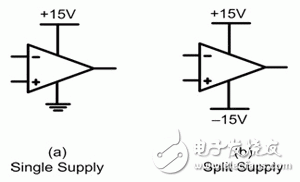
Figure 1 Op amp power supply options
Regardless of which method is used, the input common-mode voltage is determined by the supply voltage. The input common mode voltage is simply the arithmetic mean of the two voltages. Equation 1 can be used to calculate the input common-mode voltage, where VP is the value of the positive rail and VN is the value of the negative rail.
For a single-supply system, VN is always zero because the op amp's negative rail is connected to ground.
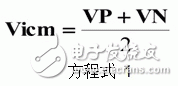
Equation 1
Using the values ​​shown in Figure 1, a single-supply op amp has a 7.5V input common-mode voltage, while a split-supply op amp has a 0V input common-mode voltage.
Some op amps can operate in a single-supply configuration or in a separate power supply configuration. Some op amps can even work with asymmetric split power supplies (VP ​​sizes are not equal to VN). In all cases, designers need to verify that the op amp can support the desired power configuration.
In addition, many op amps feature separate power supplies. Therefore, if an op amp is designed for separate supply operation in a single-supply configuration, there may be some performance differences.
When using a symmetrical separation power supply, the positive and negative voltages must be tracked to each other, especially when the circuit is first powered up. A tracking power supply is a power supply that regulates its output voltage to another voltage or signal. For most op amps, the positive supply voltage and the negative supply voltage should always be equal in magnitude and opposite in polarity.
Alternatively, you can adjust the negative supply to the same size as the positive supply and the opposite polarity. Both methods produce the same power-up waveform.
If the two supplies are not equal in magnitude and opposite in polarity, the op amp can be latched during power-up. Locking can destroy, damage, or prevent the op amp from operating properly.
Figure 2 shows a schematic of a typical op amp power supply circuit. Here, a switching power supply provides a positive 18V and a negative 18V. Two low dropout (LDO) linear regulators further adjust ±18V to ±15V. The LDO is typically mounted between the power supply and the op amp to reduce the high frequency switching noise generated by the switching power supply. LDO has a high power supply rejection (in ratio, PSRR) that reduces the noise of the LDO input at wideband frequencies.
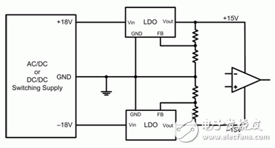
Figure 2 Typical power supply structure of an operational amplifier (click on image to enlarge)
This helps provide a low noise power supply to the op amp. The op amp also has its own PSRR, which is typically above 80dB. However, op amps have high PSRR only over a few kilohertz bandwidth, so LDOs are used to provide high PSRR up to hundreds of kilohertz bandwidth.
The circuit shown in Figure 2 does not have tracking capability. During power-up, there is no guarantee that each LDO will be the same size and opposite polarity to another LDO. The output voltage of each LDO during power-up is determined by all soft-start circuits, current limit, load capacitance, load current, and input voltage.
Therefore, it is possible that the two voltages are different in magnitude and the polarity is not opposite at the time of startup. In addition, after the LDOs are powered up and provide a steady-state DC output, they may still vary in size because each LDO has its own output voltage accuracy and the feedback resistors are slightly different due to their tolerances.
In addition to the locking problem during power-up, if the final operating DC voltage of each power supply changes over time, the power supply can affect system performance. The power supply output will vary depending on line voltage, load current changes, and temperature variations. The power output will vary within its accuracy specifications, typically 3% to 5% of the rated output voltage.
Although these supply voltage variations are small, they change the input common-mode voltage point of the op amp, which is typically modeled as an additional compensation voltage for the op amp input. Because the op amp has a high PSRR, the modeled compensation voltage is equal to the input common-mode voltage change divided by the op amp's PSRR. Equation 2 can be used to calculate the compensation voltage of the op amp input caused by the power supply change.
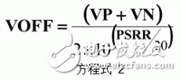
Equation 2
The PSRR shown in Equation 2 is expressed in decibels and can be found in most op amp product specifications. Equation 2 gives the compensation voltage referenced to the op amp input. The result of Equation 2 is multiplied by the op amp gain, and the op amp output can be referenced to the compensation voltage.
Since the op amp's PSRR further reduces small variations in the power supply, you may mistakenly conclude that small changes in the supply voltage have little or no effect on the system. As a quantitative example, we can analyze a fully differential op amp that buffers the signal to a 24-bit ADC.
Figure 3 shows a simplified schematic of a fully differential op amp, such as the OPA1632, which is configured as a unity-gain buffer that provides a signal to a 24-bit ADC such as the ADS1271. This circuit is a simplified schematic of the ADC evaluation board. The op amp is powered by the LDO and has a line-to-line, load, and temperature accuracy of 3%. The output voltage of the LDO is configured for a nominal value of ±15V.
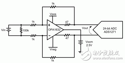
Figure 3 Example circuit for calculating the effect of compensation error (click on image to enlarge)
If the output voltage of each LDO is exactly +15V and -15V, then the common mode input voltage is just 0V. For this example, if zero volts is on its input, we read zero counts from the ADC. Then, if the power supplies are equal in size and there is no signal on the op amp input, you will read the zero count from the ADC.
However, assuming a 3% increase in positive voltage LDO output, the LDO specification is still not exceeded. With a 15V output, this 3% change is equivalent to a rise in the supply voltage from 450mV to 15.45V. According to the data sheet, the typical PSRR of an op amp is 97dB.
Equation 2 can now be used to calculate the offset voltage of the op amp input. There is an additional 3.178μV offset voltage at the op amp input. Since the op amp is configured as a unity-gain buffer, the 3.178μV is also present at the output and is applied to the ADC. The ADC's full-scale input range is ±2.5V, so each ADC bit is equivalent to 298nV.
Using the compensation voltage generated by the power supply, the ADC now reads 11 counts instead of zero counts. The power supply introduces a DC compensation error in the read ADC count. This error will vary depending on the LDO output voltage, which in turn varies with time, temperature, load current, and input voltage. This makes it difficult to remove this error by calibration and also makes the lower four bits of the ADC undefined.
An easy way to improve LDO tracking and accuracy (or drift) performance is to modify the circuit shown in Figure 2 to the circuit shown in Figure 4. The additional amplifier U1 and the four resistors need to be configured for 2 gains. Under the rated conditions, the node between R3 and R4 should be zero volts. Therefore, the value of R1 must be equal to R2, and the value of R3 must be equal to R4.
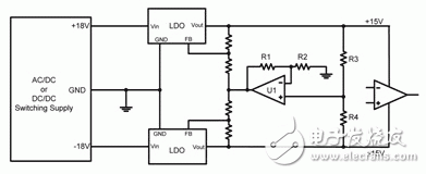
Figure 4 adds the tracked circuit. (click on the image to enlarge)
In Figure 2, the feedback network for each LDO is connected to ground. In Figure 4, the feedback resistor is connected to ground and is driven by the output of U1. Now, if any power supply changes its output voltage, the difference appears on the non-inverting input of U1 and is boosted by a factor of two. Since the output of U1 drives both LDO feedback networks simultaneously, the two LDOs are simultaneously calibrated to force their outputs to be equal in size.
The circuit shown in Figure 4 must be observed. The output of U1 can be driven to a voltage close to or equal to the power rail of U1. If the input source's ±18V is used to power U1, the output can be driven up to 18V. This 18V output is applied to the feedback pin of the LDO, which may exceed its absolute maximum voltage rating. We can add a clamping diode to protect the LDO feedback pin during high dynamic load conditions of the LDO, during short-circuit conditions, or during power-up.
Figure 5 shows a schematic of an LDO with a tracking circuit and a protection diode. To make the schematic easier to understand, the 10 μF bypass capacitors for each U3 rail have been removed.
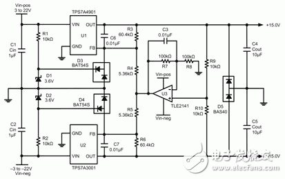
Figure 5 LDO tracking circuit with voltage protection
The circuit shown in Figure 5 uses an adjustable, negative output voltage LDO linear regulator such as the TPS7A3001 and an adjustable, positive output voltage LDO such as the TPS7A4901. U3, R7-R10 and C3 are all added components for tracking. R1, R2, D1-D5 are add-on components that control the voltage at the feedback pin to within the absolute maximum voltage range rated by their respective product specifications.
All other components are typically used to support LDOs such as input and output capacitors and feedback resistors. The LDO shown supports an input voltage range of ±36V, but due to the recommended voltage limit of the TLE2141 op amp, the input voltage to this circuit is reduced to ±22V. Higher voltage op amps can be selected to cover the LDO's full ±36V input range.
In both LDO feedback control schemes, the tracking circuit forms an additional voltage loop. The bandwidth of the added op amp U3 needs to be reduced by C3 to maintain system stability. The U3 bandwidth needs to be at least 1/10 of the lowest LDO voltage loop. This means that U3 typically only has a few kilohertz of bandwidth. Therefore, it will not be added to the system's high frequency PSRR. The PSRR of the LDO primarily determines the high frequency PSRR of the system.
The discussion in this article clearly illustrates how the DC bias supply affects some of the performance parameters of the op amp. Using the equations provided in this paper, the magnitude of these effects can be measured and calculated to determine their impact in the simulated system. In addition, you can also learn that adding some additional components to build a tracking power supply for the op amp can reduce the input compensation voltage, can establish the correct sequence to reduce the locking problem, and can also improve the DC bias power supply for the operational amplifier. The overall voltage accuracy of the linear regulator.
What is a fiber optic slip ring?
A fiber optic slip ring is a device that allows for the transfer of data, power, and signals between two rotating objects. The ring is made up of one or more optical fibers that are used to transmit light signals. These signals can be used to send power, data, or other signals between the two objects. The fiber optic slip ring is a newer technology that has many benefits over traditional slip rings.
How do fiber optic slip rings work?
A fiber optic slip ring is a device that allows electric current and optical signals to pass through a rotating joint. This is often used in applications where it is necessary to transfer data or power between two stationary points while the object rotates. The fiber optic slip ring uses light rather than metal to conduct these signals, which makes it ideal for use in high-speed or hazardous environments.
Types of fiber optic slip rings
When it comes to telecommunications, fiber optics are king. They're the backbone of almost every network today, and they're getting faster and more reliable all the time. That's thanks in part to a technology called fiber optic slip rings.
Advantages of fiber optic slip rings
A fiber optic slip ring is a device used in optical communication. It is a component of many fiber optic networks and it allows for the transmission of data over long distances without losing signal quality. Fiber optic slip rings are also used to improve the performance of other optical systems.
Disadvantages of fiber optic slip rings
Fiber optic slip rings are growing in popularity for rotating applications. Fiber optic slip rings provide many advantages over traditional electrical slip rings, including much smaller size, weight, and power consumption. However, fiber optic slip rings also have a few disadvantages. One disadvantage is that they can be more expensive than traditional electrical slip rings. Additionally, fiber optic cables are more fragile than electrical cables, so they can be more susceptible to damage.
Conclusion: What are the benefits and drawbacks of fiber optic slip rings?
When it comes to fiber optic slip rings, there are both benefits and drawbacks to consider. On the one hand, fiber optic slip rings offer a number of advantages over traditional metal contact slip rings. They are lighter in weight, which makes them easier to install and transport. They also generate less heat, making them safer to use in hazardous environments. Additionally, they provide superior performance in terms of electrical noise and signal integrity.
However, fiber optic slip rings also have some drawbacks. They are more expensive than traditional metal contact slip rings, and they can be more difficult to repair if they malfunction. Additionally, they may not be suitable for some applications due to their limited range of motion.
Fiber Optic Slip Ring,Brass Slip Ring,Fiber Optic Silp Ring,Electrical Rotary Joint
Dongguan Oubaibo Technology Co., Ltd. , https://www.sliprobs.com