Due to its high brightness, wide viewing angle, long life, and high performance-to-price ratio, LED video displays can display various texts, graphics, and images synchronously with a computer, and can play video signals such as TV, video, and video discs in real time, and can be instantly input and edited. The advantages of such multimedia data have made it widely used in many public places such as streets, plazas, commercial centers, sports venues, entertainment venues, and control centers. However, due to technical problems, the large video display also faces severe challenges, mainly in the low gray level, serious brightness loss, and low refresh rate. In addition, the video signal source in this article comes from the DVI (Digital Video InteRFace) interface. The DVI interface outputs a digital video signal. The amount of information is large. Generally, it is buffered by an external RAM (Random Array Memory), and then the video signal is processed by the processor. deal with. There are many types of external memories that can be used for digital image storage, such as SRAM, DRAM, and SDRAM, which vary in capacity and speed. DRAM and SDRAM belong to the dynamic memory, the capacity is large, need to refresh in use, when the processor does not have the external dynamic RAM interface, need to design the refresh circuit, this brings inconvenience to the system application; SRAM does not need to refresh, does not need the special-purpose interface, real-time Yes, and address jump addressing is possible, so this article uses SRAM as an external cache memory. The use of sub-field division storage technology, so that the refresh rate is greatly improved, the image display effect is clear and stable, to achieve a resolution of 800 & TImes; 256, the refresh rate of 90 Hz, red, green and blue color 256 & 256; 256 & 256; 256 gray level video display system . At the same time, with this technology, the brightness and gray level are easily adjustable, and the brightness loss is small.
2 system components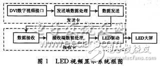
The overall block diagram of the LED video display system is shown in Figure 1. The system is composed of two parts: sending and receiving. The function of the sending part is mainly encoding and decoding the video signal transmitted by the DVI interface to form 24 b true color video data and dot clock (CLK ), Horizontal synchronization signal (HS), vertical synchronization signal (VS), data valid signal (DE) and other control signals are transmitted to receiving card through LVDS (Low Voltage Differental Signaling) level and transmitted to the receiving card through data processing. Has a specific drive structure (1/8 scan mode, 74HC595 driver chip) rhyme LED screen. This article focuses on the data processing module of the receiving card.
3 Data processing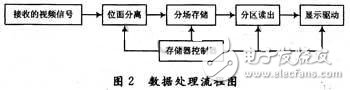
The data processing flow is shown in Figure 2. The receiving card receives the video signal (control signal and data signal) transmitted by the sending card, separates the data in the video signal through the bit plane, stores the data in the external buffer, and then reads out the partition. Sent to the display driver screen. The bit plane separation module recombines the same power bits of different data into new data stored in the memory. The external cache uses two SRAM ping-pong buffers to implement data pipeline processing. The following introduces the principle and implementation of bit plane splitting module and split-field partitioning storage.
3.1 Plane separation module
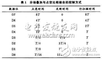
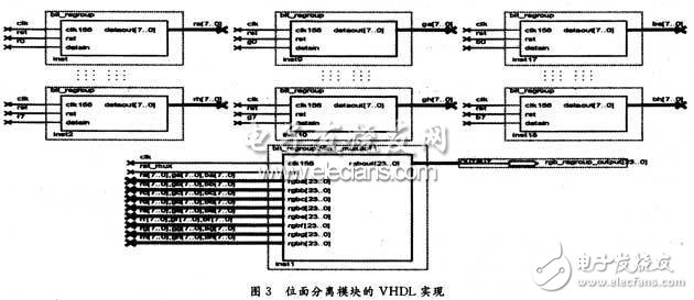
The gray-scale control method adopted in the video display screen is a combination of the sub-field superposition and the duty ratio, as shown in Table 1. The sub-field superposition means that different gray levels are achieved by constant-frequency scanning with different fields, such as Table 1 D7 ~ D4; Duty cycle control refers to control the lighting time and off-time duty cycle to achieve the adjustment of gray scale, as shown in Table 1 of D3 ~ D0. The premise of these two methods is to achieve the plane separation of video data. The plane separation is realized by FPGA. It consists of two modules, data shift register and data selector. The principle block diagram realized with VHDL is shown in Fig. 3, where r0-7, g0-7, b0-7 are the red, green and blue colors of the true color image data, respectively occupying one byte. The 24-bit data lines are registered through an 8-bit wide data shift register and then output to the external buffer through a color bit selector. Bit plane separation is achieved by controlling the address of the buffer, the data width of the external buffer is 24 bits, and the RGB three colors are used to perform bit plane separation in parallel. Among them, the shift register uses a pipelined technique. While latching and outputting the same data bits of the first eight data, it shifts into the same bit of the ninth data, which improves the efficiency of data processing.
3.2 Segmented storage
After the data is separated by bit planes, the same bits of different data form new data. By controlling the address of the memory, the same power bit of all data in one frame is written in the same segment of the memory, so the requirement for the write address generator is relatively high. . The system requires 256 shades of gray, then the memory is divided into 8 segments, each segment storing bits (fields) representing the same weight. Among them, 8 segments are replaced by 3 (23) address lines, and there are 256 lines and 800 columns for a large screen with a resolution of 800*256. Then, the line addresses are represented by 8 (28) address lines, which are 8 address lines. The first 5 bits are the zone address (32 zone), and the last 3 bits are the address of a zone (1/8 scan). The column address is represented by 7 (27) address lines, because the memory is 24 bits wide, and a memory cell represents the same power of 8 RGB points of the LED display. The order of priority from high to low is: Field Address column Address" row address. Respectively using a counter to achieve, the three counters cascaded to form the memory write address, the connection method is: field address (A17 ~ A15), area address (A14 ~ A10), the area of ​​the row address (A9 ~ A7), Column address (A6 ~ A0). It can be seen that split (8 fields) storage can be achieved by changing the priority of memory address lines.
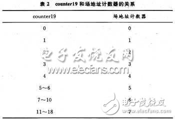
The data is written into the memory in 8 fields. When read out, 19 fields are required to be read, and the display time of each field is controlled. Therefore, when generating a field address counter for a read address, a counter 19 (0 to 18) of a 19-ary counter is designed. Table 2 shows the relationship between counter 19 and the field address counter: The display time of each field is implemented by a comparator, and the gray scale and brightness can be flexibly corrected by changing the value in the comparator.
The LED display requires that the 32 zones be lit at the same time, adopt parallel processing of data, and reduce hardware consumption and system operating frequency. Increase the refresh rate. Since the memory can only read one data at a time, it is necessary to use the partition latch and then output the 32-bit data in parallel.
The row address and the column address are the same as the write address generator. Here, they mainly describe their priorities. The data is already plane-separated, so if you want to achieve 32-zone data display at the same time, then the priority of the zone address should be the highest, followed by the column address, then the row address, and finally the field address. The connection to the memory is the same as the write address.
4 Simulation waveforms
The simulation waveform of the plane separation module is shown in Fig. 4. Among them, RGBdin[23..16] is the upper eight bits of the input data, and rgb_regroup_output[23..16] is the upper eight bits of the output data. Flag is the input data valid signal flag, and flag_delay85 is the output valid signal flag.
The waveform analysis is as follows:
Input data before the first 8 data are 00h, 8th is 02h, the 8 data after the plane separation output see Table 3, from Table 3 can be seen that the plane separation achieved the first 8 data transfer Read from right to left after setting it.
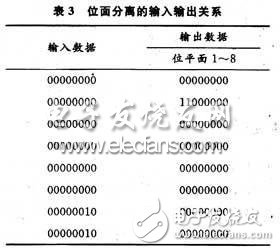
Figure 5 shows the simulation waveform of the write address. It can be seen that the field address has the highest priority. When the field address is 7h, the column address is incremented by 1. When the column address is 63h, the row address is incremented by 1. When the row address is 7h, the area address is plus 1. Similarly, it can be seen that the carry order of the read address in FIG. 6 is: when the area address is 1Fh, the column address is incremented by 1, the column address is 63h, the row address is incremented by 1, and the row address is 7h, the field address is counted according to the 19 field principle. . When the row address in Figure 6 is 7h, the field address is not incremented by one. Figure 7 shows the duty cycle signal controlled by the field address counter. This signal is connected to the enable end of the display driver board trace signal, and the gray scale is achieved by controlling the scan signal to control the display time.

Aiming at the problem of the refresh speed and grayscale control encountered in the system of LED video display screen, this paper presents a split-area partitioned storage technology, and introduces its principle and implementation in detail. Through waveform simulation and engineering application, this method can well solve the problem of image flicker and brightness loss in LED display control system, and its gray and brightness control can be flexibly corrected.
Focusing on the development and production of Wireless Charging products that make life easier.
Supply various wireless charger including multifunctional Wireless Charger, Car Wireless Charger, Magnetic Wireless Chargin, Wireless Charging Mouse Pad, etc.
We help 200+ customers create custom wireless charging products design for various industries.
Manufacturing high quality products for customers according to international standards, such as CE ROHS FCC REACH UL SGS BQB etc.
Wireless Charging Pad,Wireless Phone Charger,Wireless Car Charger,Bluetooth Charger
TOPNOTCH INTERNATIONAL GROUP LIMITED , https://www.itopnoobluetoothes.com