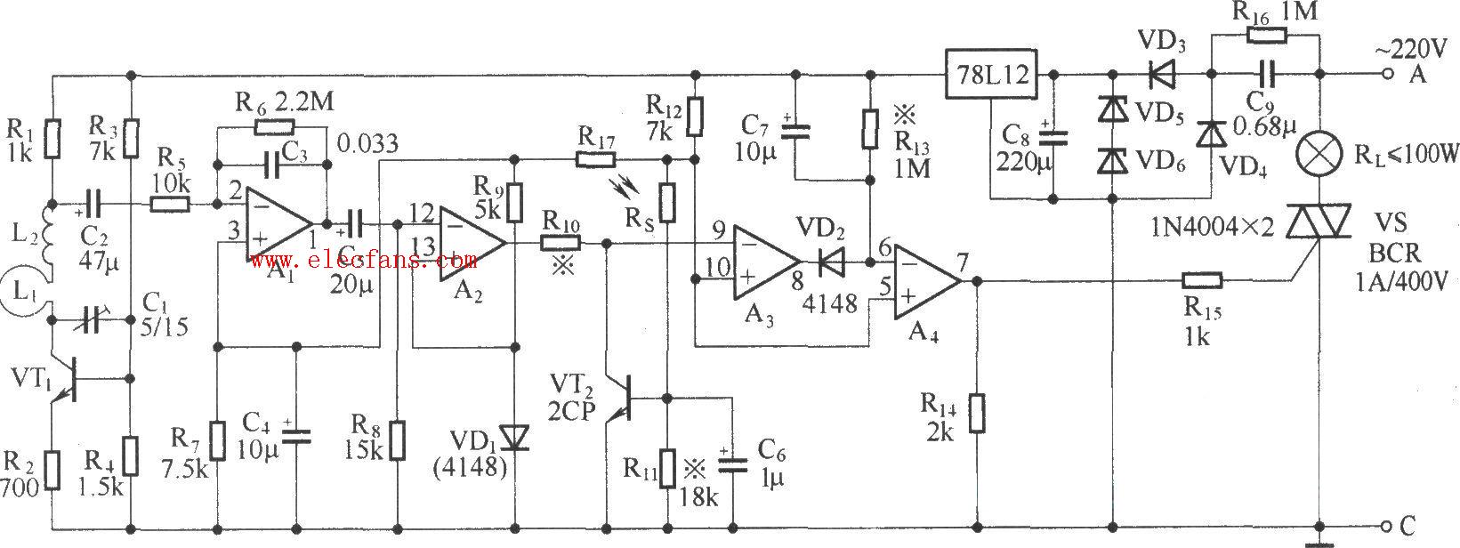
Schematic of delay circuit 1:
The radar-type energy-saving lamp holder is essentially a human body microwave sensor switch. When someone walks into the effective range, the electric lamp automatically lights up and turns off automatically after a delay. If the human body has been moving in this range, the electric lamp continues Lit. The radar-type energy-saving lamp also has a light control function, so that the electric lamp only works at night. The picture is the circuit diagram of the radar-type energy-saving lamp holder:
Schematic diagram of delay circuit 2:
Infrared remote control delay lamp Infrared remote control delay lamp is suitable for temporary situations at night. This kind of lighting does not need to be turned off by the remote control after it is turned on by the remote control, but is automatically turned off after a delay through the delay circuit set in the circuit. The delay time can generally be set to 1 "2MIN, and its operation can use the infrared remote control transmitter without the modulation signal that has been introduced before. Circuit schematic diagram:
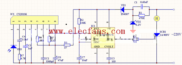
Circuit principle: The circuit is composed of an infrared receiver, a monostable delay circuit and a thyristor circuit. As shown in the figure, the infrared receiver circuit is composed of CX20160A and photodiode VD. In this circuit, the center frequency of the IC has been set to f0 = 40khz by the band-pass filter center frequency setting resistor R, which is basically applicable to most infrared remote control transmitters. When the photodiode VD receives the transmission signal from the transmitter, the output pin 7 of the IC outputs a low level. In the monostable delay circuit, a pulse-start monostable trigger is composed of a 555 circuit and RP, C, which is triggered by a negative pulse or low level through 2 feet to make it flip. Normally, because pin 7 of the IC outputs a high level, pin 3 of the IC outputs a low level. When pin 7 of the IC outputs a low level, IC2 is turned over by pin 2, and pin 3 becomes a high level. This high level triggers the thyristor VS through R to make it conductive and the electric lamp is on. The monostable circuit is triggered to flip and enter the temporary stable state. At this time, the power is charged to C through RP. The time required for C to charge is the delay time of the monostable trigger. This time TD = 1.1RPC5. Due to the use of adjustable resistance RP, the transient stability time of the monostable circuit can be adjusted as needed. When C5 is charged and its positive terminal voltage rises to 2VDD / 3, the monostable circuit reverses, the 3 pin of the IC returns to low level, the bidirectional thyristor VS is turned off, and the light goes out. Selection and production of components: VD2 should use 6.2V voltage stabilizing diode, SCR1 uses 1A / 400V unidirectional thyristor or bidirectional thyristor, and other components have no special requirements. Installation and debugging: Component installation: resistance, adjustable resistance, capacitance, MIC, triode, inductance L, IC Debugging method: After the components are installed correctly, power on for debugging. The debugging is mainly divided into two parts, one is the monostable delay circuit composed of 555. Measure the voltage between pins 4, 8 and 1 of IC555 before power-on debugging. The voltage should be 6V. When the voltage changes, VD1, VD2, C1, R1 should be checked. The key point is to check whether VD2 is damaged. When checking this part of the circuit Be very careful, or you will give 220V AC power down. When debugging the 555 monostable delay circuit, touch the second pin of IC2 with a test pen, then the lamp H will light up. If it doesn't work, check the circuit of IC2 for errors. The values ​​of R2 and C7 determine the length of the delay time. The second part is the infrared receiving circuit composed of IC1 CX20106. The infrared signal is input from pin 1 of IC1 and output from pin 7. R4 is the setting resistance of the center frequency of the band-pass filter, and the receiving frequency of the receiver can be changed by changing its resistance. C4 and R7 determine the amplification gain. The total gain of IC1 is designed to be 77 "79dB. Under this gain, the pulse amplitude output from pin 7 of IC1 is about 3.5" 5V. C2 is an integral capacitor, and its capacity is generally 330PF. When C2 is large, although the anti-interference ability can be improved, it also increases the low-level duration of the output pulse, resulting in a shorter remote control distance.
COVID-19 continues to have an enormous impact on global tourism and air travel as people have been homebound. Closed destinations and hotels and restrictions on travel, camping, and outdoor recreational activities will impact travel and tourism. According to the World Tourism Organization (UNWTO), as of April 2020, all tourist destinations worldwide have introduced travel restrictions, 97 destinations (45%) have totally or partially closed their borders for tourists, 65 destinations (30%) have totally or partially suspended international flights, and 39 destinations (18%) are closing borders by banning the entry of passengers from specific countries of origin. COVID-19 has impacted regions such as Asia Pacific, Europe, Middle East, and North America. The above restrictions have directly impacted the portable power station market globally.
Portable Energy Storage Device,Portable Energy Storage Outlet,Battery Energy Storage System,Solar Battery Storage System Cost
Shenzhen Zhifu New Energy Co., Ltd. , https://www.sunbeambattery.com