This article describes the main features of the dsPIC33F family, a series of product block diagrams and a 220W solar microinverter reference design for the grid, including key features and specifications, reference design block diagrams, design board schematics, and bill of materials (BOM).
The dsPIC33F family is a high-performance 16-bit digital signal controller (DSC) with a modified Harvard architecture and C compiler optimized instruction set with 16-bit wide data bus and 24-bit wide instructions, operating at 40MIPS at 3.0-3.6V Suitable for multi-loop switching power supplies (SMPS) and other digital power converters such as AC/DC converters, DC/DC converters, power factor correction (PFC), uninterruptible power supplies (UPS), inverters, embedded power control And digital lighting, etc.
Key features of high performance 16-bit digital signal controller:
The scope of work:
• Operating speeds of up to 40 MIPS (at 3.0-3.6V):
- Industrial temperature range (-40°C to +85°C)
- Extended temperature range (-40°C to +125°C)
High-performance Digital Signal Controller (DSC) CPU:
• Improved Harvard Architecture
• C compiler optimization instruction set
• 16-bit wide data bus
• 24-bit wide instructions
• Linear program memory space that can address up to 4M instruction words
• Addressable linear data storage space of up to 64 KB
• 83 basic instructions: mostly single word / single cycle instruction
• Two 40-bit accumulators with rounding and saturation options
• Flexible and powerful addressing modes:
- Indirect addressing
- Modular addressing
- Bit reversal addressing
• Software stack
• 16 x 16-bit fractional/integer multiplication
• 32/16-bit and 16/16-bit division operations
• Single Cycle Multiply - Accumulate:
- Accumulator write back operation for DSP operations
- Double data fetch operation
• Up to 40 bits of data can be shifted left or right by up to 16 bits
Digital I/O:
• Peripheral pin selection
• Up to 35 programmable digital I/O pins
• Wake-up/level change interrupt function on up to 30 pins
• Output pin can drive voltages from 3.0V to 3.6V
• Open-drain configuration, up to 5V output
• Digital input pin can withstand 5V (except RB5)
• The pull/sink current for all PWM pins is 16 mA on-chip flash and SRAM:
• Flash program memory (up to 16 KB)
• Data SRAM (up to 2 KB)
• Boot and general security peripheral features of the Flash program memory:
• Timer/Counter, up to 3 16-bit timers
- Can be paired up to 1 32-bit timer
• Input capture (up to 2 channels):
- Rising edge capture, falling edge capture or rising/falling edge capture
- 16-bit capture input function
- Each capture channel has a 4-level depth FIFO buffer
• Output comparison (up to 2 channels):
- Single or double 16-bit comparison mode
- 16-bit glitchless PWM mode
• 4-wire SPI:
- Frame support and I/O interface for simple codecs
- Level 1 depth FIFO buffer
- Support for 8-bit and 16-bit data
- Supports all serial clock formats and sampling modes
• I2CTM:
- Support for full multi-master slave mode
- 7-bit and 10-bit addressing
- Bus collision detection and arbitration
- Integrated signal conditioning
- slave address mask
• UART:
- An interrupt is generated when an address bit is detected
- An interrupt occurs when a UART error occurs
- wake up the device from sleep mode when the start bit is detected
- 4-character deep send and receive FIFO buffers
- LIN bus support
- Hardware IrDA® encoding and decoding
- High speed baud rate mode
- Hardware flow control using CTS and RTS
Interrupt controller:
• Interrupt response delay is 5 cycles
• 118 interrupt vectors
• Up to 35 interrupt sources
• Up to 3 external interrupts
• 7 programmable priorities
• 4 processor exceptions
High Speed ​​PWM Module Features:
• Supports up to 4 PWM generators and provides 4-8 outputs
• Each of the eight PWM outputs has an independent time base and duty cycle
• Dead and falling edge dead zones
• Duty cycle resolution is 1.04 ns
• Dead zone resolution is 1.04 ns
• Phase shift resolution is 1.04 ns
• Frequency resolution is 1.04 ns
• Supported PWM modes:
- Standard edge alignment
- True independent output
- Complementary
- Center alignment
- Push-pull
- Multiphase
- Variable phase
- Fixed off time
- Current reset
- Limiting
• Independent fault/current limit input for 8 PWM outputs
• Output override control
• Special event triggers
• PWM capture function
• Input clock prescaler
• Dual trigger signal sent by the PWM module to the ADC (analog-to-digital converter, ADC)
• PWMxL and PWMxH output pin swap
• PWM4H and PWM4L pins are remappable
• PWM frequency, duty cycle and phase shift can be changed during operation
• Prohibition of each independent PWM generator
• Leading-Edge Blanking (LEB) function high speed analog comparator
• Up to 4 analog comparators:
- 20 ns response time
- 10-bit DAC associated with each analog comparator
- DACOUT pin providing DAC output
- Programmable output polarity
- Optional input source
- ADC sampling and conversion function
• Interface to the PWM module:
- PWM duty cycle control
- PWM cycle control
- PWM fault detection
High speed 10-bit ADC
• 10-bit resolution
• Up to 12 input channels can form 6 conversion pairs
• Two internal reference voltage monitoring inputs form a pair of internal analog inputs
• Successive ApproximaTIon Register (SAR) converter for parallel conversion of analog input pairs:
- For devices with two SARs, the conversion rate is 4 Msps
- For devices with one SAR, the conversion rate is 2 Msps
• Dedicated result buffer for each analog channel
• Independent trigger source for each analog input conversion pair
Power management:
• On-chip 2.5V regulator
• Real-time clock source switching
• Idle, hibernate and hiccup mode for fast wake-up
CMOS flash technology:
• Low-power high-speed flash technology
• Fully static design
• 3.3V (±10%) operating voltage
• Industrial and extended temperature
• Low power consumption
System Management:
• Flexible clock selection:
- External oscillator, crystal, resonator and internal RC oscillator
- Phase-Locked Loop (PLL) with 120 MHz Voltage Controlled Oscillator (VCO)
- Primary crystal oscillator in the range of 3 MHz to 40 MHz
- Internal low power RC (Low-Power RC, LPRC) oscillator with a frequency of 32 kHz
- Internal fast RC (Fast RC, FRC) oscillator with a frequency of 7.37 MHz
• Power-on Reset (POR)
• Brown-out Reset (BOR)
• Power-up TIMER (PWRT)
• Oscillator Start-up TImer (OST)
• Watchdog timer with its own RC oscillator
• Fail-Safe Clock Monitor (FSCM)
• Multiple reset sources
• In-Circuit Serial ProgrammingTM (ICSPTM)
Package:
• 18-pin SOIC
• 28-pin SPDIP/SOIC/QFN-S
• 44-pin TQFP/QFN 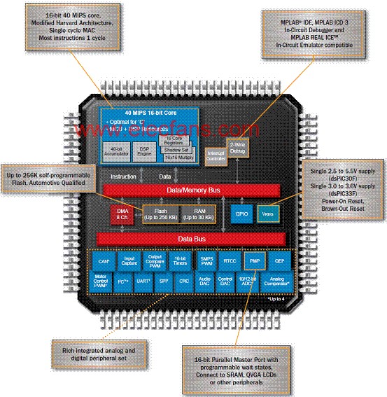
figure 1. dsPIC33F Series Product Block Diagram
Solar micro-inverter reference design for grid connection
Grid-Connected Solar Micro Inverter Reference Design
This reference design demonstrates the flexibility and power of SMPS dsPIC® Digital Signal Controllers in Grid connected power conversion systems. This reference design works with any photovoltaic (PV) panel of maximum 220 Watts having open circuit voltage between 25V to 55V DC. This reference design Two maximum of this reference design is available to support 110V and 220V Grid. 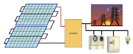
figure 2. Solar energy series block diagram for connecting to the grid
This reference design is implemented using a single dsPIC33F "GS" digital-power DSCs from Microchip that provides the full digital control of the power conversion and system management funcTIons. As shown in this reference design the dsPIC33F 'GS' devices enable designers to easily and Cost effective create products using advanced switching techniques that lower switching losses and enable efficiencies as high as 95%. Grid-Connected Solar Micro Inverter Reference Design is royalty free when used in accordance with the licensing agreement.
Main features of the solar micro-inverter reference design connected to the grid:
Peak efficiency of 95%
Output current THD < 5%
Power factor >0.95
Maximum power point tracking
Grid voltage and frequency tracking
Protection against various current and voltage faults
Night time power consumption <1W
System Islanding to detect grid failure
Full Digital Control
Reference design indicators for solar micro-inverters connected to the grid:
Micro Inverter for individual PV Module up to 220W
Wide PV Panel voltage : 25V to 55V DC
Maximum Power Point Tracking voltage: 25V to 45V
Maximum DC short circuit current : 10A
Grid Frequency range :
47 – 53 Hz for 220V systems
57 – 63 Hz for 110V systems
Grid voltage range :
90V – 140V for 110V systems
180V – 264V for 220V systems
230V solar micro inverter system indicators:
• Maximum output power = 185 watt
• Nominal output voltage = 230V
• Nominal output current = 0.8A
• Output voltage range = 180 VAC-264 VAC
• Output frequency nominal frequency = 50 Hz
• Output frequency range = 47 Hz-53 Hz
• Power factor = >0.95
• Total harmonic distortion = <5%
• Efficiency
- Peak efficiency = 95%
- Maximum Power Point tracking = 99.5%
- Minimum efficiency>0.8
110V solar micro inverter system indicators:
• Maximum output power = 185 watt
• Nominal output voltage = 110V
• Nominal output current = 1.7A
• Output voltage range = 90 VAC-140 VAC
• Output frequency nominal frequency = 60 Hz
• Output frequency range = 57 Hz-63 Hz
• Power factor = >0.95
• Total harmonic distortion = <2% 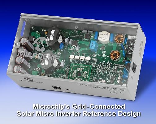
image 3. Solar micro-inverter reference design outline drawing connected to the grid 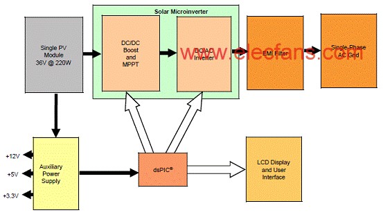
Figure 4. Solar micro-inverter reference design block diagram for connecting to the grid (1) 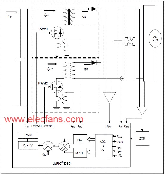
Figure 5. Solar micro-inverter reference design block diagram for connecting to the grid (2) 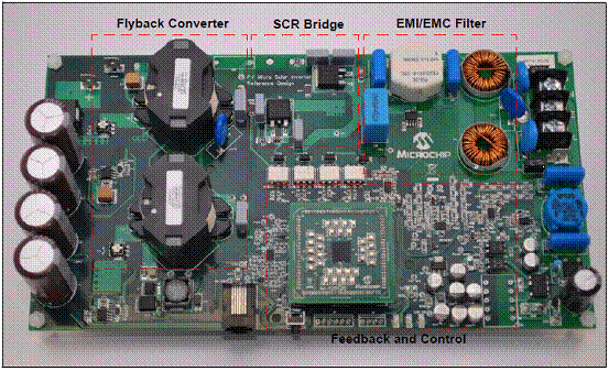
Figure 6. Solar micro-inverter reference design board outline drawing connected to the grid 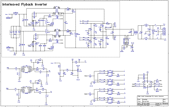
Figure 7. Solar micro-inverter reference design board circuit diagram for connecting to the grid (1) 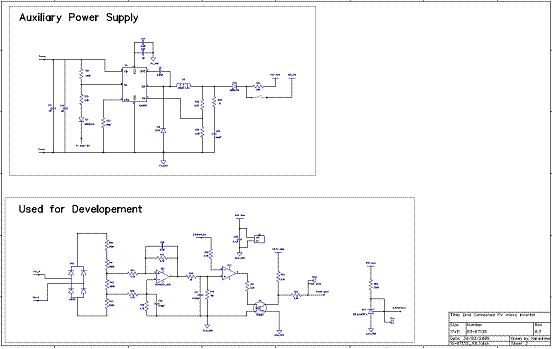
Figure 8. Solar micro-inverter reference design board circuit diagram for connecting to the grid (2) 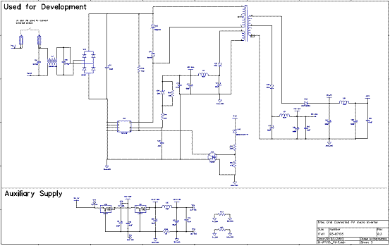
Figure 9. Solar micro-inverter reference design board circuit diagram for connecting to the grid (3) 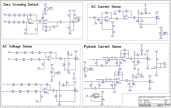
Figure 10. Solar micro-inverter reference design board circuit diagram for connecting to the grid (4) 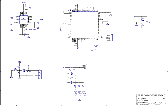
Figure 11. Solar micro-inverter reference design board circuit diagram for connecting to the grid (5)
- [Worldwide Compatibility]With a worldwide 100-240V AC input, it's a truly global charger and perfect for international traveling. Compatible with iOS, Android, & Windows smart phones as well as tablets, speakers, cameras, and other 5V USB devices
-
With 9 years experience in the filed, Shenzhen WAWEIS Technology Co., Ltd is one of the best power supply device manufacturer in China. Our world-class production plant passed ISO9001:2008 & ISO14001:2004 certifications and is equipped with the state-of-art technology and machines. The main products we make are power adapters, which can be used in laptop, LCD display, LED lights, CCTV camera(12v series), Speaker(24v series), Balance car(42v series). All our products comply with European environmental standard as well as CCC,RoHS ,CE , FCC.
Ungrouped,High Quality Ungrouped,Ungrouped Details, CN
Shenzhen Waweis Technology Co., Ltd. , https://www.waweispowerasdapter.com