Electromagnetic interference is caused by signal currents in large loops.
Figure 9.6 illustrates an ordinary electromagnetic interference problem. A 64-bit bus is connected from board A through connector B to the motherboard. The motherboard may be a main CPU card or a passive channel to other daughter cards. The return current of the 64 signal lines flows back from the motherboard C to the board A, and most of them pass through the grounding legs of the connector B.
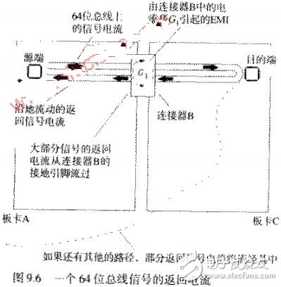
Only a small fraction of the signal return current flows back to board A via a different path. However, it is this small portion of the return current that causes a large number of EMI problems.
When a high-frequency current flows through a large loop, a large amount of electromagnetic energy is radiated, which will not pass the radiation test specified by FCC or VDE. The main job of EMI design is to minimize the area of ​​the current loop cross section for all signals. For example, on a complete ground plane, the high-frequency current tends to return just below the trace, a 6IN long, and the loop from the ground plane of 0.010IN surrounds the loop area of ​​only 0.006IN. Such a large loop area is acceptable in terms of EMI. In Figure 9.6, the 64-bit bus signals on boards A and C are returned by the full ground plane, so we can ignore the loop area between their signal and ground.
Any blocking or discontinuity in the return current path, such as a transition on the connector ground pin, creates a "bubble" on the current loop that will cause a large enough area, causing the radiation to exceed the standard, depending on The total DI/DT value of the signal current in the loop.
In Figure 9.6, the bubble on the loop area typically occurs in connector B because the signal on the connector and the ground pin are separate. This bubble is denoted as G1, and the loop inductance of the 64-bit bus signal path is mostly derived from the inductance of the loop G1.
Whether the signal return current has other return paths depends on the physical structure of connector B and the specific structure of the chassis in which boards A and C are located. Any current that returns to the source on board A will not contain connector B and will contain a large loop area and generate a large amount of radiation.
For example, in Figure 9.7, it is assumed that boards A and C share two connectors, and the additional connectors are denoted as D, which are arranged at a distance from connector B. Now the return current of a part of the signal can be added by the ground line on connector D, as shown by loop G2 in Figure 9.7.
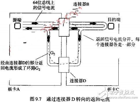
Adjusting the ratio of the return current of the signal through connector D depends on the ratio of the inductance of loop G1 (see Figure 9.6) to the inductance of G2 (see Figure 9.7):
![]() (Formula 5)
(Formula 5)
At very low frequencies, the amount of signal return current flowing through connector D depends on the ratio of impedance, while at higher frequencies it depends on the ratio of the inductance in the above equation. Now that EMI is a high frequency problem, here we only care about the ratio of the inductance of the two loops.
Because the area of ​​the loop G1 is small, its inductance is also smaller than that of the G2, so only a small portion of the return signal current passes through the path G2. However, even such a small portion of the current is sufficient to cause the radiation to exceed the standard. Above 30 MHZ, testing is performed at a distance of 3 M from the device, and the radiation limits of both FCC and VDE are approximately 100 UV/M. For more details on radiation standards and design techniques to prevent electromagnetic radiation, reference is made to the OTT, MARDIGUIAN and KEISER et al.
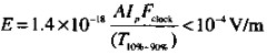
It is unrealistic to accurately calculate the radiation intensity level of a digital product because there are too many factors that can affect the result. The following equation represents a simple constraint: open measurement test, above 30MHZ, loop area, peak current and rise time that meet FCC and VDE radiation limits.
 (Formula 6)
Among them: E=3M national radiation electric field intensity, V/M
A = radiation loop area, IN2
IP=peak current, A
T10~90%=Signal rise time
FCKOCK=Time Frequency, HZ
Note on the above formula:
It is common for the final product's radiation index to differ from the budgeted estimate of the above formula by 20DB, including a large correction factor.
It should be clear that the radiation test is the sum of all the line radiation in the test system. If a line just meets the standard, then adding 100 lines will definitely not meet the standard.
Before designing the final settings, set up an analog system test, which only needs to include some clock signals through the connector system, which sounds wasteful, but in the end it will save a lot of money. The cost increases dramatically as the mechanical packaging and shielding needs to be redesigned at the end of the project.
ZGAR PCC
ZGAR electronic cigarette uses high-tech R&D, food grade disposable pod device and high-quality raw material. All package designs are Original IP. Our designer team is from Hong Kong. We have very high requirements for product quality, flavors taste and packaging design. The E-liquid is imported, materials are food grade, and assembly plant is medical-grade dust-free workshops.
From production to packaging, the whole system of tracking, efficient and orderly process, achieving daily efficient output. We pay attention to the details of each process control. The first class dust-free production workshop has passed the GMP food and drug production standard certification, ensuring quality and safety. We choose the products with a traceability system, which can not only effectively track and trace all kinds of data, but also ensure good product quality.
We offer best price, high quality Vape Device, E-Cigarette Vape Pen, Disposable Device Vape,Vape Pen Atomizer, Electronic cigarette to all over the world.
Much Better Vaping Experience!


ZGAR PCC E-Cigarette Vape Pen,ZGAR PCC Device Vape,ZGAR PCC Vape Pen Atomizer,Latest Disposable E-Cigarette OEM vape pen,ZGAR PCC electronic cigarette
Zgar International (M) SDN BHD , https://www.zgarvapor.com