When the combined logic that generates the gated clock exceeds one level, the reliability of the design project becomes difficult. Even if the prototype or simulation results do not show a static danger, there may still be dangers. In general, we should not use multi-level combinatorial logic to clock the flip-flops in a PLD design. Figure 7 shows an example of a multi-level clock with a dangerous image. The clock is output by a multiplexer controlled by the SEL pin. The input to the multiplexer is the clock (CLK) and the divide by 2 (DIV2) of the clock. As seen from the timing waveform diagram of Fig. 7, in the case where both clocks are logic 1, when the state of the SEL line changes, there is a static danger. The extent of the danger depends on the conditions of the job. The danger of multi-level logic can be removed.
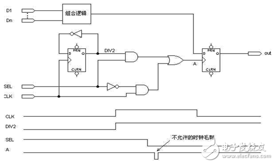
Figure 7 Multi-level clock with static danger
Figure 8 shows an alternative to a single stage clock of the Figure 7 circuit. The SEL pin and DIV2 signal in the figure are used to enable the enable input of the D flip-flop instead of the clock pin for the flip-flop. The use of this circuit does not require the logic unit of the additional PLD, but the work is much more reliable. Different systems require different methods to remove multi-level clocks, and there is no fixed mode.
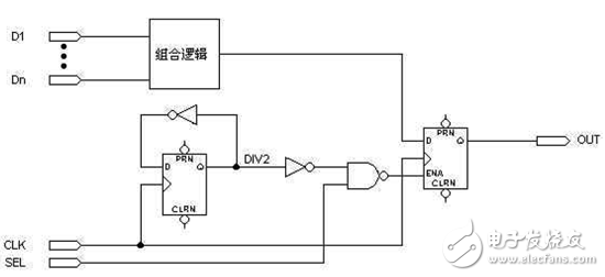
Figure 8 Multi-level clock without static danger
Traveling wave clock
Another popular clock circuit uses a traveling wave clock, where the output of one flip-flop is used as the clock input for the other flip-flop. If carefully designed, the traveling wave clock can work as reliably as a global clock. However, the traveling wave clock complicates the circuit-related timing calculations. The traveling wave clock generates a large time offset between the clocks of the flip-flops on the traveling wave chain, and will exceed the worst-case setup time, hold time, and clock-to-output delay in the circuit, making the actual system The speed is decreasing.
When using an inverted flip-type flip-flop to form an asynchronous counter, a traveling wave clock is often used. The output of one flip-flop clocks the input of the next flip-flop. Referring to Figure 9, the synchronous counter is usually a better alternative to the asynchronous counter, because both require There are also many macrocells and the sync counter has a faster clock to output time. Figure 10 shows a synchronous counter with a global clock, which has the same function as Figure 9, with the same number of logic units, but with a faster clock-to-output time. Almost all PLD development software offers a wide variety of sync counters.
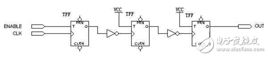
Figure 9 Traveling Wave Clock
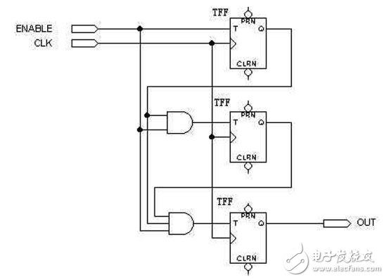
Figure 10 The traveling wave clock is converted into a global clock
This charging station including charring station for PS5, PS4,Xbox series X, Nintendo Switch. For PS5 we have many design, fasting charging,LED light indicator, also with Type C adapter , you can choose any one you like.
for the Nintendo Switch , we have multi functional for gamepad, console, joycons and game carde storeges, we also have 4 in 1 joycons charging dock fast charging!
All docking we accept OEM/ODM order, we can 100% ensure the quality and offer you good After-sales service.


Controller Charging Station,Dualsense Charging Station,Charging Dock,Controller Charging Dock
Shenzhen GEME electronics Co,.Ltd , https://www.gemeelectparts.com