A special method for obtaining positive and negative power in a single power supply circuit. The core device of the polarity conversion circuit shown in Figure 1 is a normal non-gate. Since the input terminal and the output terminal are shorted together, the output voltage of the NOT gate is equal to the input voltage (Vi=VO); thus, the NOT gate is forced to operate at the center point of the transfer characteristic curve, so the output voltage is limited to The threshold level of the gate circuit is equal to half the power supply voltage. If we use the output of the NOT gate as the DC ground terminal, we can convert the power supply voltage VCC to a dual supply voltage of ±VCC/2; It acts as a regulator that stores current, and the output impedance of the circuit is low, so the output voltage is also stable.
The non-gates in the figure can be used with common gate circuits such as 74HC00 or CD4069. Considering the limited ability of CMOS non-gate drive loads, it is best to use several non-gates in parallel to increase their effective output current. Capacitors C1 and C2 in the figure. Decoupling, the capacity can be appropriately larger. 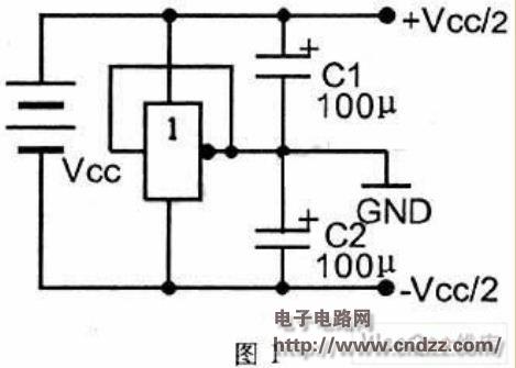
In the circuit shown in Figure 2, the non-inverting input terminal of the op amp is connected with a symmetrical series resistor divider, and the op amp itself is connected in the form of a voltage follower. According to the linear operation of the op amp, it is easy to see that the output of the op amp is The potentials between the partial pressure points are strictly equal. Since the output of the op amp is grounded, the power supply VCC of the op amp is divided into two sets of symmetric positive and negative power supplies ±VCC/2. 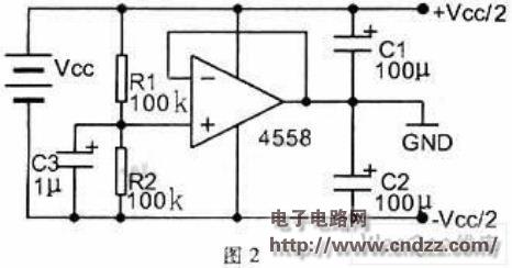
When the output current of the op amp can not meet the actual demand, it can't be used in parallel as the gate circuit is simple; in this case, the general-purpose low-power op amp can be replaced by a power amplifier-type op amp device with a large output current, such as the common TDA2030A. Similar to Figure 1, C1 and C2 are both decoupling capacitors, and the capacitor C3 of the non-inverting output of the op amp acts to suppress interference and filtering. For most OTL power amplifiers, the internal symmetry is generally set. According to the above principle, we can completely convert the single power supply into two-polar positive and negative power supplies of equal size. The specific circuit is shown in Figure 3. Shown. 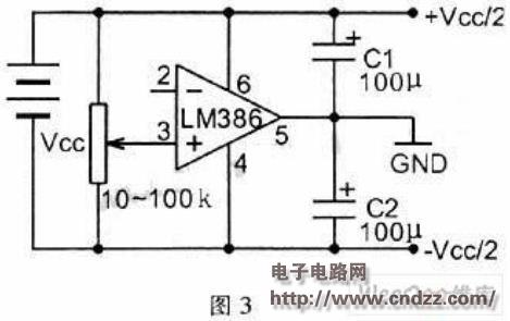
In fact, due to the discreteness of the content parameters and the influence of the bootstrap circuit structure, the voltage at the output of the set is not absolutely VCC/2, which causes the positive and negative output voltages to be unbalanced. For this we need to connect a 10-100kΩ potentiometer between the positive and negative sources, and connect the LM386 pin 3 input to the center tap of the potentiometer, while the second pin remains floating. After the above improvements are made to the circuit, by adjusting the DC input level of the power amplifier, positive and negative voltage values ​​of very close size can be obtained at the output end of the chip.
[More items]
electrical current monitoring sensors,dc current monitoring sensor,dc current monitor,current sensor board
Shanghai Zhilong Electronic Technology Co.,Ltd , https://www.zhilongsensor.com