Capacitive loads are not easily driven at high speeds. The fundamental reason is that the current charging speed due to voltage changes is limited only by the equivalent series resistance (ESR), which is often very small in modern multilayer capacitors. Another reason is that if we connect the capacitor to the feedback control system, the pole introduced by the capacitor can cause phase loss. This pole forces us to limit our bandwidth to well below our expectations, so as not to affect stability. Therefore, if we want to produce clear and controlled upper and lower edges on a capacitive load, we need a "buffer" with a wide bandwidth and a large current, and it can neither oscillate nor occupy too much volume to occupy your work. Half of the space in the station.
The method described below uses very few components to achieve small size and minimizes functional loss, and can be easily added back when needed. The circuit described here, called LineEdge2, produces high-speed upper and lower edges when connected to high-load DC and capacitive loads. This circuit is widely used in Dialog Semiconductor for line transient response, PSRR and other performance measurements to aid in the characterization of power management ICs.
Modern power management ICs include linear and switching converters that are integrated with the digital core. The digital core can be a hard-coded large state machine or a software-driven micro CPU. All converters must meet the specifications of the maximum voltage variation range to ensure proper operation during load or line transients. A typical method of measuring this parameter requires a power amplifier to provide a step change to the input of the converter, while an electronic load is applied to the output of the converter to provide the specified load, and an oscilloscope (to measure input conditions and output deviation). The complete setup is shown in Figure 1.
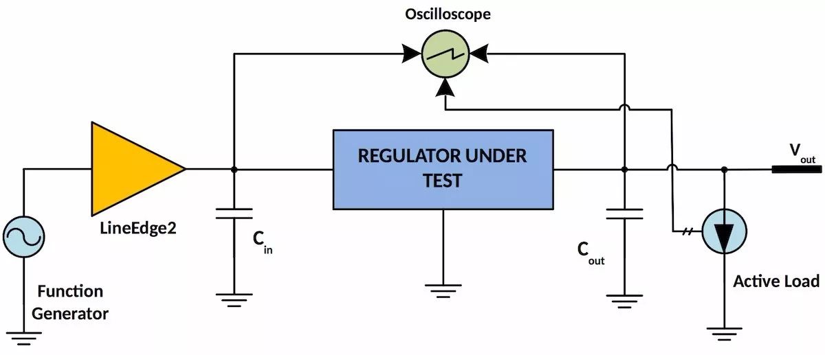
Figure 1. Line transient response measurement setup
An easy way for many novice engineers is to use a Coaxial Cable to connect the power amplifier to the input capacitor of the target board. Power amplifiers often cannot withstand such capacitive loads. In most cases, the input of the converter becomes an oscillator and can even cause damage to the input capacitor or the converter itself. The usual solution is therefore to change the coaxial cable to short and series resistors to isolate the amplifier from the capacitive load. This can make it stable, but the isolation resistance affects the accuracy of the amplitude. And because it is used with the input capacitance of the regulator, a low-pass filter is generated, which reduces the bandwidth.
One might ask: Why can't the capacitor be completely removed and only the power amplifier is used to drive the device under test (DUT)? This method causes the switching type DC-DC converter to be unstable. In addition, if the digital core is also powered from the same power supply, it can cause frequent digital core resets and instability. One compromise is to reduce the value of the input capacitor to a low enough level to allow it to drive both the stability of the regulator. However, this solution requires additional experimentation and results in a system with a different hardware configuration than the original design, which is not desirable from an application or design perspective.
What if I want to design a circuit that can drive a large capacitive load? This requires a high bandwidth amplifier plus compensation scheme to address the phase loss problem caused by the load capacitance. After several experiments with fly wires and prototype PCBs, LineEdge was born, and after a series of improvements, LineEdge2 was created.
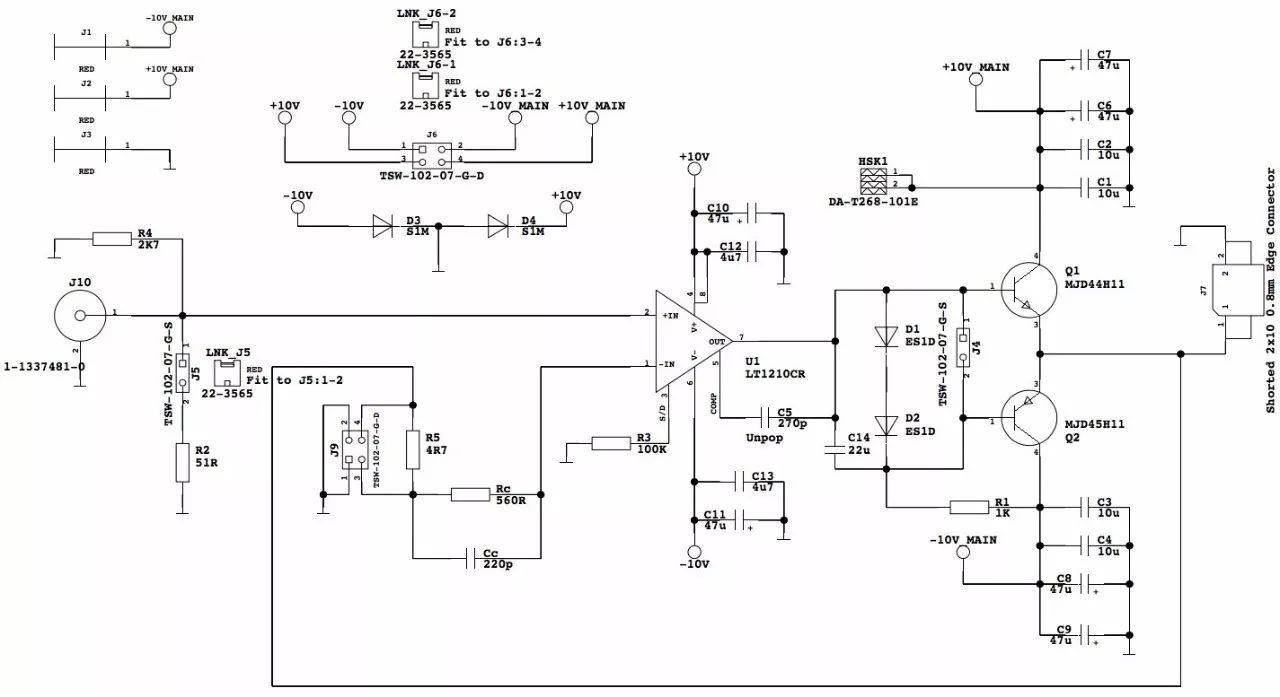
Figure 2. LineEdge2 schematic
As can be seen from the schematic, LineEdge2 consists of a current feedback amplifier (CFA) U1 (LT1210), a basic bias network, and a BJT output stage (Q1 and Q2). The LT1210 is an interesting amplifier; it has a high current output (> 1A) and a high bandwidth (35 MHz), and its default design is to drive "high" capacitive loads (up to 10nF). In order to effectively utilize the high current of the amplifier, its output is directly connected to the base of the NPN bipolar transistor Q1. This arrangement is reasonable because LineEdge2 always operates with a positive output voltage. The output stage uses a complementary high switching speed power transistor with an hFE of approximately 50 to provide sufficient current amplification. Since most of the current actually flows through the component, the NPN transistor adds additional cooling. The PNP is biased by two diode voltage drops, and the transistor current is transmitted with a collector current of approximately 10 mA, allowing the output to operate in Class AB. This offset is indeed very simple, as it is only necessary for the PNP to be slightly opened in the case of a light output load.
When the load is high, the output stage enters class A, and the PNP hardly opens. To improve the PNP drive when fast upstream and downstream edges are required, a bootstrap capacitor is placed in parallel with the bias diode. This can provide energy to the base briefly on the falling edge of the transient response. If the device is used in a low power scenario, it is inverted by a shorted link to a Class B output. The main reason for using the AB class for output is to avoid cross-over distortion, which would otherwise generate additional high-frequency noise. The collectors of the two transistors are heavily decoupled to provide local power when needed.
Please note that there is no emitter resistance in the schematic. The emitter resistance helps to mitigate the thermal runaway risk of the PNP, but it also increases the amplifier driver swing requirements and increases the supply voltage requirements due to the extra voltage drop. Therefore, in order to ensure that the output stage does not have thermal runaway, the appropriate bias resistor value is set in the circuit and the diode is thermally coupled to the PNP. A 100kΩ resistor in series with the SD (off) pin is used to reduce power consumption, but the total bandwidth of the CFA is also slightly reduced. The compensation of capacitive loads is very simple. The CC is connected in parallel with the RC to set the bandwidth of the CFA. R5 is a injection resistor for loop testing, which together with J9 facilitates stability measurements. The input signal is directly connected to the forward high impedance input with an optional 50Ω termination impedance. C5 is connected to the CFA's compensation pin. Since it does not help improve performance in this application, it is not connected to this component.
stability
Typical capacitive loads driven by LineEdge2 range from 10μF to 100μF. Depending on the type and capacity of the capacitor, it may be necessary to fine tune the phase margin. Figure 3 shows two extreme capacitive loads. The gain loss due to the capacitive load is obvious, and it appears that the impedance characteristics of the capacitor will cut into a portion of the expected first order gain roll off. A higher capacitance value has a lower resonant frequency, forcing the first crossing to occur earlier. Capacitors with lower capacitances have higher quality factors, and a steeper valley occurs after crossing at higher frequencies. The phase begins to recover at the resonant frequency and quickly jumps to the high value of the design in the amplifier. Obviously, we have two intersections and two phase margins. In this case, all intersections need to be considered and stability will be subject to the "weakest link" or the smallest phase margin. In this case, the weakest link will always be the first intersection determined by the load capacitor. In order to stabilize the system, we have two options: either to increase the gain in some way to avoid the first intersection, or to advance the phase (at a lower frequency), to ensure that there is still some phase at the first intersection. . To increase the gain, simply reduce the RC value, or to increase the phase, simply increase the CC. Figure 3 shows two cases with a fixed value of RC = 560 Ω and two CC values. It is clear that the 820pF case provides better phase margin under both capacitive loads.
It is worth mentioning that the load is interesting and significant phase margin modulation. Figure 4 depicts the situation of different load points under low capacitive loads. As the gain increases, the phase change is very small. The increase in gain results in a higher crossover frequency, and as the phase rises rapidly after the crossover, the phase margin also rises accordingly. Obviously as the load increases, the phase is also increasing, while gain and bandwidth are also increased. As a result, as the load increases, faster speed and higher stability are obtained. As shown, when the load differs by 400 mA, the phase margin changes by 10°.
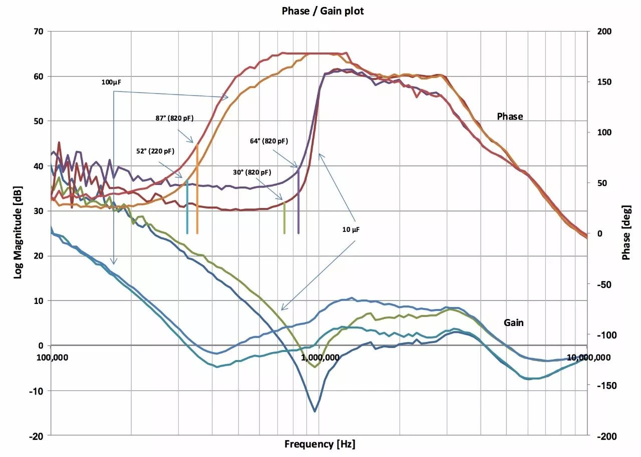
Figure 3. Phase margin map with 10μF and 100μF capacitive loads
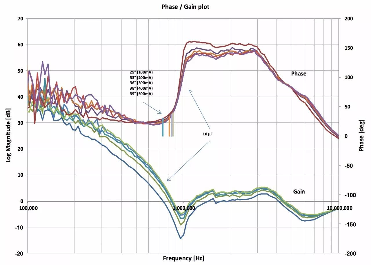
Figure 4. Phase margin map at different load points
automation
LineEdge2 is a simple device that does not contain any additional protection or current limiting circuitry. It can be used stand-alone or as part of a larger automation system with many independent power outputs.
Since line transient response is measured at full load, heat dissipation can be an issue. To solve this problem, the load transient pulse is applied synchronously with the input pulse and ensures that the output voltage has proper pre- and post-settling times. As a result, the converter's load is not constant, but pulsed, with a small duty cycle, which reduces the loss of the LineEdge and DUT. Figure 5 shows the pulse arrangement. The blue curve is the input transient driven by LineEdge2 and the yellow curve is the load transient pulse. The input transient pulse is in the middle of the load transient pulse with sufficient time margin to stabilize the output voltage – the red curve. Obviously, in order to achieve this pulse arrangement, the function generator for the standard stage may not be sufficient because the phase synchronization of the two pulses must be controlled and the pulse width and slope must also be controlled. The image also shows the line pulse's superior pulse fidelity with virtually no cross-over distortion, overshoot or undershoot, and the pulse actually shows the waveform of the function generator. By reducing the repetition rate of the pulse arrangement, the total power loss can be reduced, so the heat sink is no longer needed, making the solution small and easy to integrate. As can be seen from Figure 5, the line transient response of the regulator is very small (red waveform synchronized with the line transient pulse) - about 1 mV, so the measurement signal should be specially protected from interference from other noise sources.
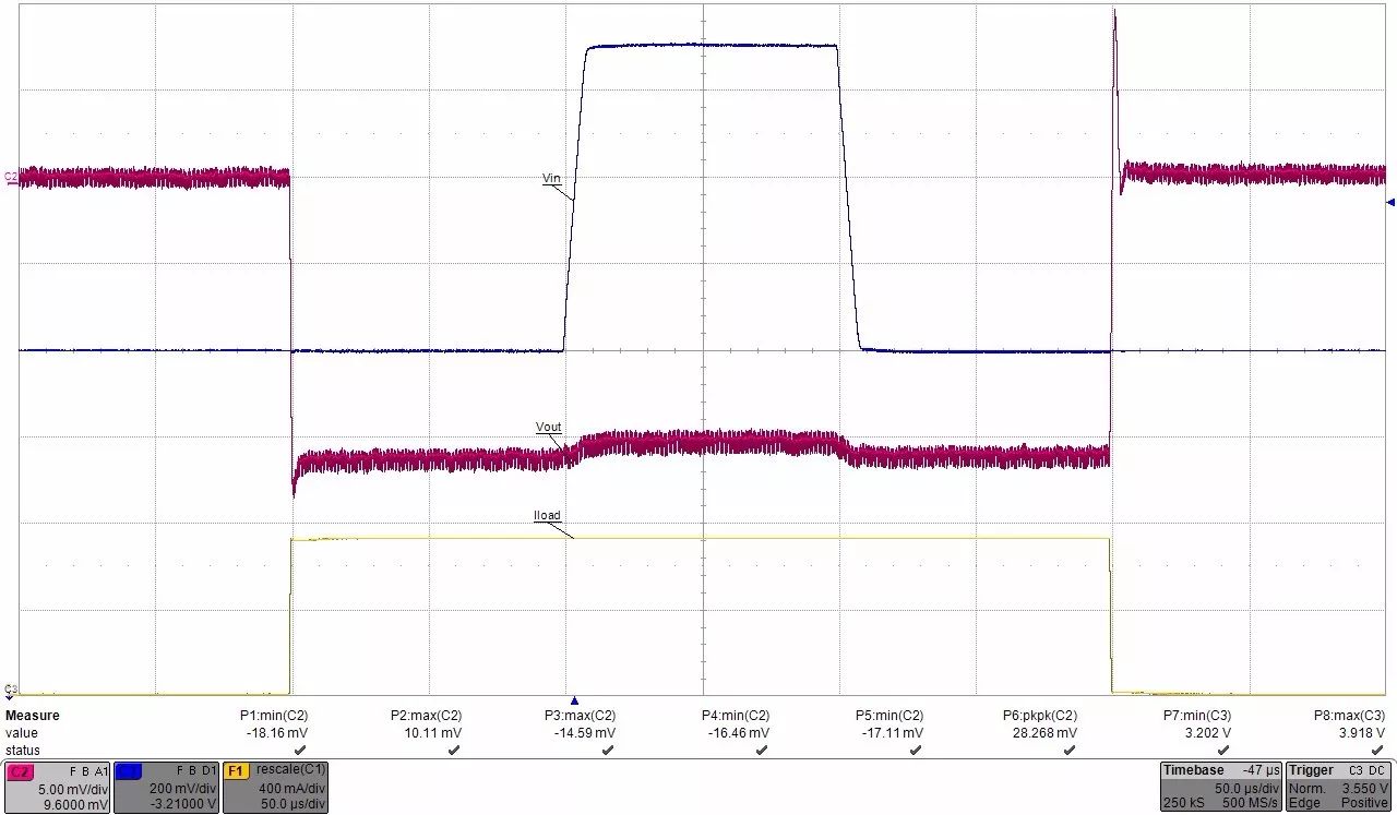
Figure 5. Line transient response automation
hardware
The implemented LineEdge2 is a small module that can be plugged directly into the target evaluation board. As shown in Figure 6, it uses a high-speed, high-current Samtec HSEC8 connector to connect to the target system, which can be matched near the input capacitance to allow the LineEdge2 board to be inserted from the top. It is very important that the board needs to be connected as close as possible to the input capacitor. There are several reasons. First, for a large current static load, the connection resistor will generate a voltage drop. Since the feedback of the main amplifier is connected to the board end, some voltage drop may be seen at the input end. Second, the impedance in the connection limits the speed and ability to charge the capacitor, resulting in poor signal fidelity. Therefore, usually we put the connector in the desired position when making the motherboard.
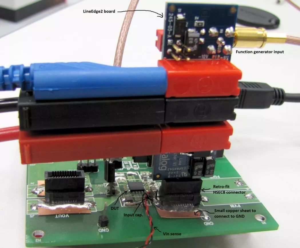
Figure 6. Setting up with the modified HSEC8 connector
in conclusion
As an application engineer at Dialog, we often need to perform complex measurements and provide results in a short period of time. Having the right tools, knowing and knowing how to use it will bring indispensable advantages and greatly reduce the complexity of the task. LineEdge2 is one such tool that is widely used within Dialog to assist in the measurement and characterization of complex PMICs.
Cat 5 Cable Wiring,Cat 5E Ethernet,Shielded Cat5E Cable,Cat5E Outdoor Cable
Zhejiang Wanma Tianyi Communication Wire & Cable Co., Ltd. , https://www.zjwmty.com