The microwave circuit usually has a high frequency (above 1 GHz), and is a planar circuit formed by a microstrip transmission line of a microwave integrated circuit device, and the entire structure can be easily fabricated on a dielectric sheet by a thick and thin process regardless of the complexity of the pattern. It is fixed to a metal base (carrier) as a ground plate to form a complete circuit. The cost of making such a circuit is much less expensive than the waveguide and coaxial circuits of the same function. This kind of circuit has been widely used because it eliminates many joints and brings advantages such as good repeatability, excellent performance, convenient adjustment, small size, light weight and high reliability.
Microwave circuit fabrication can generally be divided into three stages. The microwave device is fabricated → the substrate microstrip line is fabricated and composed of functional blocks → connected with the metal base to form a microwave circuit. Due to the high frequency of operation, the microwave circuit has a particularly high grounding requirement. The grounding includes the grounding of the functional block substrate and the ground connection of the functional block and the metal base. In particular, the latter, the conventional screw connection, causes crosstalk between functional blocks (generally ≥ 0.5 dB) due to the gap between the connections, and the insertion loss increases (generally ≥ 1.4 dB), which also brings additional capacitance and oscillation. The circuit above the L-band has been unable to obtain stable circuit parameters and has low reliability. At present, the brazing method has been widely used in foreign countries to implement "large-area brazing". Domestically, it has also begun to explore and use. The main difficulty in large-area brazing is that the physical and chemical properties of metal and ceramic materials are too different, which may cause ceramic cracking, poor joints, deformation, and the like. The length of the chip and the microstrip line interconnect, the degree of camber, the precision of the microstrip line fabrication, etc. are also factors that affect the microwave performance. This article mainly introduces the research results of the author and colleagues in this regard.
1 Analysis and design of ground connectionsThe ground connection of the microwave circuit mainly affects the circuit crosstalk and insertion loss. Circuit crosstalk is mainly caused by excessively long connecting lines forming additional inductance. Insertion loss is mainly composed of four parts: conductor loss, dielectric loss, radiation loss, and loss of manufacturing process.
Conductor loss refers to the metal conduction band and the grounded metal facing the transmission signal
The resulting insertion loss. Dielectric loss refers to the insertion loss introduced by the filling medium by the electromagnetic field transmitted in the medium between the metal conduction band and the ground plane. Welding defects (cavities, voids) and other manufacturing defects (medium plates, conduction bands) increase the insertion loss [1]. The design principle of the ground connection is to be grounded nearby and a large area (full area) is grounded. Several typical grounding methods are:
(1) Grounding metallized through hole: Mainly connected to the microstrip line and the ground plane of the substrate. It can be realized by hole metallization, hollow rivets, and connecting pins. As shown in Figure 1.
Ground via design
Hollow rivet
Connecting pin
Figure 1 Several typical grounding methods
(a) Film grounding hole - perimeter metallization
(b) Thick film grounding hole - full hole metallization
(c) Multi-layer thick film, large-area grounding,
The mesh holes are used and the holes are metallized.
Each of the three methods has its own technical difficulties, especially the thin film metallization hole, which is still in the research stage, with a success rate of only 90%. The method of using hollow rivets is the most reliable, but the manufacture of hollow rivets is more difficult.
(2) Grounding edging: In order to connect the grounding surface to a larger area, the copper foil (thickness 0.10 to 0.20 mm) connecting surface can be used if conditions permit. as shown in picture 2.
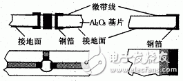
Figure 2 Schematic diagram of the grounding
The grounding of the edging is relatively reliable, but only in the place where the aperture and the sideband are large, and the welding work is often performed manually, requiring the operator to be highly skilled.
(3) Large-area welding of grounding surface and grounding plate: Large-area welding used to replace screw connection is the main means to ensure reliable grounding.
The transmission line (microstrip line) in the microwave circuit is usually fabricated by a thin film process (evaporation, sputtering, ...) on a solid dielectric substrate (ceramic, quartz, ...). With the development of new technologies, the microwave circuit microstrip line is also made of thick film and LTCC (low temperature co-fired ceramic) technology. In recent years, non-Al2O3 soft substrate composites have also appeared as substrates, but above the S band, Often it is not a substitute for ceramic materials.
The connection between the ceramic material and the grounding plate metal, that is, the connection between the grounding surface and the grounding plate. Conventional screw connection, in addition to the assembly and use of the ceramic substrate is likely to cause fragmentation, it can not meet the electrical and thermal performance parameters of microwave circuits, has been replaced by soldering technology in recent years.
Due to the great difference in chemical and physical weldability between ceramics and metals, the difference in thermal expansion coefficient causes cracking of the ceramic plates and failure of the circuit during soldering and use. The study of these issues will be described in Sections 2 and 3.
2 Welding performance researchWhen the ceramic substrate is soldered to the metal pedestal, the ceramic metallization (thin, thick film process) and the characteristics of the MIC device are often used to achieve the soldering method. The grounding surface of the ceramic substrate and the carrier must have excellent soldering properties.
(1) Metallization of the ground plane of the substrate
The main way to metallize the microwave circuit substrate is through film, thick film and LCTT co-firing.
(a) Film production
The microwave film circuit generally uses a CrAu film system. The Cr layer acts as a transition layer to improve the adhesion strength of the metal to the ceramic plate, and Au serves as the main layer to meet the requirements of microwave electrical performance.
The Au-based solder can be used to weld the CrAu film to the carrier. However, the Au-based solder is expensive and must be carried out in a special gas-controlled furnace. The process is complicated. To study the metal film suitable for ordinary Sn-Pb solder. system.
Three membrane systems of CrAu, CrCuAu and CrAuCuAu were designed and studied, and different film thicknesses were produced by different techniques. The test results are shown in Table 1.
Smartwatch
Smartwatch,Smart Watch,Screen Touch Watch,G Shock Smart Watch
everyone enjoys luck , https://www.eeluck.com