At present, many universities and research institutes have conducted research on EMI (Electromagnetic Interference) of switching power supplies. Some of them are based on the mechanism of EMI generation, and some have proposed many practical and valuable solutions based on the impact of EMI. Here, several effective solutions have been analyzed and compared, and new reference suggestions for the suppression of EMI in switching power supplies have been proposed.
Electromagnetic Interference Generation Mechanism of Switching Power Supply
The interference generated by the switching power supply can be divided into two kinds: noise interference and harmonic interference. If divided by the coupling path, it can be divided into conduction interference and radiation interference. Now according to the noise interference source to explain:
1, the diode caused by the reverse recovery time interference
When the rectifier diode in the high-frequency rectifier circuit is conducting forward, a large forward current flows. When the rectifier diode is turned off due to the reverse bias voltage, there are more carriers accumulated in the PN junction, and thus the carrier current In the period before the disappearance of the child, the current will flow in the reverse direction, causing the reverse recovery current of the carrier to disappear and a large current change (di/dt) to occur.
2. Harmonic interference caused by switch operation
The power switch tube flows a large pulse current when it is turned on. For example, the input current waveforms of the forward converter, push-pull converter, and bridge converter are approximately rectangular waves when they are resistive loads, and they contain abundant high-order harmonic components. When using zero-current, zero-voltage switching, this harmonic interference will be very small. In addition, during the cut-off period of the power switch tube, the sudden change of the current caused by the leakage inductance of the high-frequency transformer winding also generates a spike.
3, interference caused by the AC input circuit
Switching power input rectifiers without power frequency transformers will cause high-frequency damping oscillations to cause interference during reverse recovery.
The peak interference and harmonic interference energy generated by the switching power supply are transmitted through the input and output lines of the switching power supply and are called conduction disturbances. The energy of harmonics and parasitic oscillations are transmitted through the input and output lines. Generate electric and magnetic fields. This kind of interference caused by electromagnetic radiation is called radiation interference.
4, other reasons
Parasitic elements of the components, the schematic design of the switching power supply is not perfect, the printed circuit board (PCB) wiring is usually hand-arranged, has a great deal of randomness, PCB near-field interference, and the installation of the device on the printed board, Placement, as well as unreasonable orientation can cause EMI interference.
Switching power EMI characteristics
As an energy conversion device operating in a switching state, the switching power supply has a high rate of change in voltage and current and generates a relatively high level of interference; the interference source is mainly concentrated during the power switch and the heat sink and the high-level transformer connected thereto, as opposed to the digital The position of the circuit disturbance source is relatively clear; the switching frequency is not high (from several tens of kilohertz and several megahertz), and the main interference forms are conducted interference and near-field interference; and printed circuit board (PCB) traces are usually manually routed. With greater randomness, this increases the difficulty of extracting PCB distribution parameters and estimating near-field interference.
EMI test technology
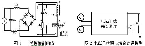
There are currently three methods for diagnosing differential mode common mode interference: RF current probes, differential mode rejection networks, and noise separation networks. The use of RF current probes is the easiest way to measure differential mode common-mode interference, but the comparison of measurement results with standard limits requires more complex scaling. The differential-mode suppression network has a simple structure (see Figure 1). The measurement results can be directly compared with the standard limits, but only common-mode interference can be measured. The noise separation network is the best method, but its key components transformer manufacturing requirements are high.
Current measures to suppress interference
The three elements that form electromagnetic interference are interference sources, propagation routes, and disturbed devices. Therefore, the suppression of electromagnetic interference should also start from these three aspects. First, interference sources should be suppressed to directly eliminate the cause of interference; secondly, the coupling and radiation between the interference source and the victim device should be eliminated, and the transmission path of electromagnetic interference should be cut off (see Figure 2); the third is to improve the immunity of the victim device. To reduce its sensitivity to noise. Currently, several measures to suppress interference are basically used to cut off the coupling channel between the electromagnetic interference source and the victim equipment. They are indeed effective methods. Commonly used methods are shielding, grounding, and filtering.
The use of shielding technology can effectively suppress the electromagnetic interference of the switching power supply. For example, power switch tubes and output diodes usually have a large power loss. In order to dissipate heat, it is often necessary to install a heat sink or mount directly on the power supply base plate. When the device is installed, it is necessary to insulate the insulating sheet with good thermal conductivity. This results in distributed capacitance between the device and the backplane and the heat sink. The bottom plate of the switching power supply is the ground of the AC power supply, and therefore the distributed capacitance between the device and the backplane. The electromagnetic interference is coupled to the AC input to generate common-mode interference. The solution to this problem is to use a shielding sheet sandwiched between the two insulating sheets and to connect the shielding sheet to the DC ground and cut off the RF interference to the input power grid. way. In order to suppress the radiation generated by the switching power supply and the influence of electromagnetic interference on other electronic devices, the shield can be completely processed in accordance with the method of shielding the magnetic field, and then the entire shield can be integrated with the casing and the ground of the system to realize the electromagnetic field. Effectively shielded. Some parts of the power supply connected to the earth can play a role in suppressing interference. For example, the grounding of the electrostatic shielding layer can suppress the interference of the changing electric field; in principle, the conductor used in the electromagnetic shielding may not be grounded, but the ungrounded shielding conductor often enhances the electrostatic coupling and generates a so-called “negative electrostatic shielding†effect, so the grounding is still good. , so that the electromagnetic shielding can also play the role of electrostatic shielding. The common reference point of the circuit is connected to the earth and provides a stable reference potential for the signal loop. Therefore, in the system, the safety ground wire, the shield ground wire and the common ground reference wire all form the grounding busbar, and finally connect with the earth.
In the design of the circuit system, the principle of “one point grounding†should be followed. If a multi-point grounding is formed, a closed ground loop will occur. When the magnetic flux passes through this loop, magnetic induction noise will be generated, and it is actually difficult to achieve “one point groundingâ€. Therefore, in order to reduce the impedance of grounding and eliminate the effect of distributed capacitance, planar or multi-point grounding is used. Using a conductive plane (a conductive plane layer of a base plate or a multi-layer printed board circuit, etc.) as a reference ground, each part of the ground is required. Nearly received the reference ground. To further reduce the voltage drop in the ground loop, a bypass capacitor can be used to reduce the magnitude of the return current. In a low-frequency and high-frequency coexistence circuit system, the ground lines of the low-frequency circuit, high-frequency circuit, and power circuit should be separately connected and then connected to a common reference point.
Filtering is a good way to suppress conducted interference. For example, if a filter is connected to the input of the power supply, it can suppress the interference generated by the switching power supply and feed it back to the grid, and it can also suppress the noise from the grid to the power supply itself. In the filter circuit, many special filter elements are also used, such as a feedthrough capacitor, a three-terminal capacitor, and a ferrite core, which can improve the filter characteristics of the circuit. Properly designing or selecting filters and properly installing and using filters is an important part of anti-jamming technology.
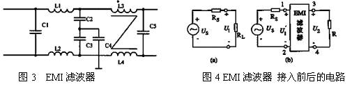
EMI filtering technology is an effective measure to suppress spike-like interference, which can filter out the conduction interference caused by various reasons. Figure 3 is an EMI filter consisting of a capacitor and an inductor connected to the input of a switching power supply. In the circuit, C1 and C5 are high-frequency bypass capacitors used to filter out differential mode interference between two input power lines; L1 and C2, C4, L2 and C3, and C4 form a common-mode interference filter to filter power. Asymmetrical common-mode interference between line and ground; L3, L4 have equal primary and secondary turns and opposite polarity. The alternating current produces the opposite magnetic flux in the core, which effectively suppresses common-mode interference. The test shows that as long as the parameters of the components are properly selected, the conduction interference generated by the switching power supply can be well suppressed.
Most of the existing suppression measures consist of eliminating the coupling and radiation between the interference source and the victim equipment, and cutting off the transmission route of electromagnetic interference. This is indeed an effective method to suppress interference, but few people involve direct control. Sources of interference, elimination of interference, or enhancement of the immunity of a victim device, but they do not know there is much room for development.
Suggestions for improvement measures
At present, the suppression of interference from the transmission of electromagnetic interference has gradually matured. Our point of view is to return to the switching power supply itself. Judging from many years of work practices, the following points must be noted in the circuit:
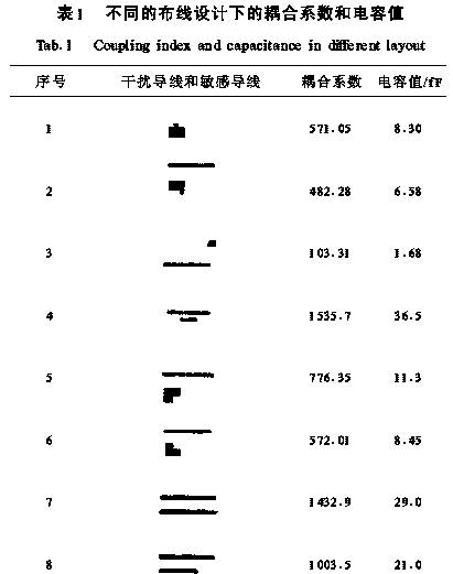
(1) In the layout of the printed circuit board, the analog circuit area and the digital circuit area should be separated reasonably, the power supply and the ground wire should be separately led, and the power supply should be converged to one point; when the PCB is routed, the high-frequency digital signal line must be short-circuited. The signal lines are preferably centered on the PCB board, and the power lines are separated as far as possible away from the high-frequency digital signal lines or ground lines. Second, the wiring can be based on the coupling factor to minimize interference coupling. (See Table 1)
(2) Printed board power lines and ground printed strips are as wide as possible to reduce the line impedance, thereby reducing the interference noise caused by the common impedance.
(3) The device uses multiple chip components and shortens the pin length of the component as much as possible to reduce the influence of the distributed inductance of the component.
(4) Connect the filter capacitor as close as possible to the device at the Vdd and Vcc supply terminals to reduce the switching current flow path, such as 10μF aluminum electrolysis and 0 1μF capacitors connected to the power supply pin. For the high-speed digital IC's power supply, a tantalum electrolytic capacitor can be used instead of an aluminum electrolytic capacitor because the impedance to ground of tantalum electrolysis is much smaller than aluminum electrolysis.
in conclusion
There are still many factors that cause electromagnetic interference in switching power supplies. There is still a lot of work to do to suppress electromagnetic interference. The comprehensive suppression of various noises of the switching power supply will make the switching power supply more widely used.
Teaching and training meetings, classroom teaching; traditional projectors are not easy to carry. In school classrooms, due to the naughty students, projectors are not safe in the classroom and are easily damaged by students. The portability of micro projectors makes up for the teaching vacancies. In the future, teachers will give lectures. You only need to store the data in the projector to show it to students for teaching, saving the trouble of textbooks and handwriting with pens and chalks.
portable projector for teaching,portable projector education,portable classroom projector,projector for teachers
Shenzhen Happybate Trading Co.,LTD , https://www.happybateprojector.com