Except for its lower end, the millimeter wavelength range (30-300GHz) has not been well utilized. New applications in imaging, security, medical treatment, and short-distance wireless transmission, as well as the ever-increasing data rate of optical fiber transmission, may quickly change this state [1], [2]. In the past thirty years, III-V technologies (GaAs and InP) have gradually expanded to this millimeter wave range. Recently, due to the continuous reduction of process size, silicon technology has joined this "game."
In this article, semiconductor active devices that can be used in 100-GHz and 100-Gb/s applications are reviewed in accordance with semiconductor characteristics and device requirements. Then the most widely used technology is introduced, followed by two competing technologies in different aspects: the frequency divider, to illustrate that the technology is suitable for use in high-speed digital circuits, and the oscillator to illustrate its application in analog circuits In performance.
Basic characteristics of materials and processes
Characteristics of semiconductor materials
The performance of electronic devices operating at very high frequencies is mainly related to: 1) the material properties of the semiconductor and 2) the structure of the device [3]. Si, GaAs and InP are currently the materials of choice for devices with cut-off frequencies of 300 GHz and above. In Table 1, people give some relevant parameters that characterize energy gap, carrier transport characteristics and thermal conductivity. The characteristics of InGaAs matched with InP, GaN and InAs lattices are also reported.
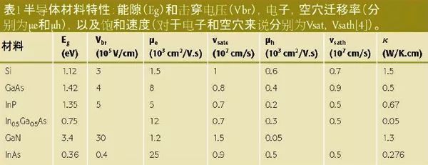
Having a sufficiently large energy gap (Eg>1eV) is very advantageous because it can provide good breakdown characteristics. Si, GaAs and InP can actually withstand voltage levels of several volts at 100nm; in addition, the pn junction shows a very clear rectification behavior, and the leakage current at room temperature is negligible. Higher breakdown voltage can be obtained by using GaN, and InAs can only be used for devices with very low voltage because of its low energy gap.
The electron mobility in III-V materials is greater than that of silicon, which means that at a given doping concentration, the n-type contact region has a lower series resistance, while for the p-type region, due to III -V materials have lower hole mobility, the opposite is true. However, the carrier velocity that controls transconductance and transit time in the high-field region of the device is close to the saturation drift velocity depending on the carrier type (Vsat or Vsath′ depends on the carrier type; close to 10nm /ps). Due to transient effects (electrons move from low energy levels in the conduction band, high mobility valleys to higher energy levels, and the conversion of low mobility valleys does not happen instantaneously), the transmission of electrons usually benefits from some overshoot; for example , The effective speed derived from the base-to-collector transition time of an InP heterojunction bipolar transistor (HBT) with a thin collector is greater than 3×107cm/s, which is about 5 times the saturation speed [5 ].
Very high frequency performance means shorter transit time and lower RC parasitics; for field effect transistors (FET) and bipolar transistors, this can usually be achieved by reducing the size of electronic devices and increasing current density Implementation (for example, see [6]). For ultra-high frequency devices and circuits, thermal conductivity becomes an important parameter. When silicon is compared with its III-V technology rivals, its good thermal conductivity becomes a real advantage because of this. It is possible to achieve higher device density.
One of the main advantages of early monolithic microwave integrated circuits (MMIC) based on III-V technology is due to the semi-insulating properties of the undoped (or compensated) substrate, which is directly related to its large semiconductor energy gap ( The resistivity of the substrate is on the order of 108Ω·cm, while the resistivity of silicon is 104Ω·cm). This makes it possible to realize resistance, inductance and transmission lines with low associated parasitic effects. With the recent development of a huge microwave application market (for example, mobile phone networks), great progress has been made in introducing passive components to silicon-based technology. In addition, insulator-loaded silicon substrate technology (SOI) has shown its potential to reduce parasitic effects (however, this comes at the expense of lower substrate thermal conductivity).
FETs and bipolar transistors for high frequency applications
Today, bipolar transistors and FETs suitable for high frequency applications are based on heterojunction structures (except for silicon-based MOSFETs). The development of heterojunctions has been for more than 40 years, and the materials and lattice stress are still being developed. The heterojunction between two different materials (having the same crystal structure and the same lattice parameters) is mainly due to their energy gap difference, and the conduction band and valence band step methods distinguished by this difference Characterized (Table 2). In the active area of ​​the transistor, the heterojunction is used for two different purposes:
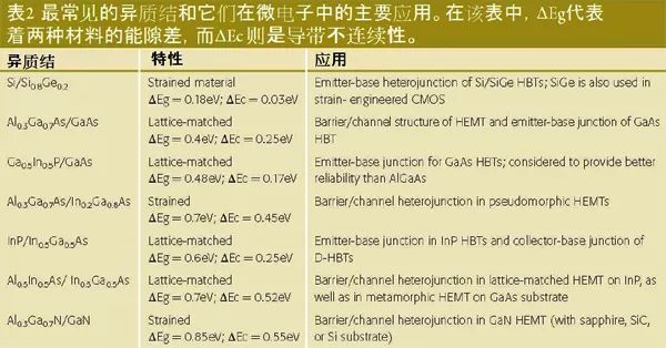
• Regardless of their respective doping concentrations, ensure that the electron-dominated carriers are injected from the emitter to the base of the bipolar transistor. • In the high electron mobility transistor (HEMT), the electrons are limited to undoped The heterogeneous quantum hydrazine.
Although it was originally implemented for lattice-matched heterojunctions, it soon showed that performance can also be enhanced when used in mismatched heterojunctions, provided that the stress crystalline layer is within the limit of the pseudocrystalline thickness (if the growth layer If it is thin enough, its lattice constant will be adjusted to that of the substrate). This characteristic is used in HBT (for example, graded-composition method) to generate a base layer with a short transit time and a channel layer with a high mobility HEMT. Above the critical thickness, (the higher the degree of mismatch, the thinner the layer thickness), the growth layer relaxes, and lattice dislocation will occur in the crystal structure. This phenomenon can still be used to generate high-quality crystal layers with different lattice parameters on the top of the substrate, with a transition layer (buffer layer) in the middle to trap most of the dislocations. For example, this structure can be found in what is called a metamorphic HEMT, where a high-quality active heterostructure is grown on top of the relaxed buffer layer. In particular, the denatured structure allows the use of extremely high mobility InAs channels [7], [8].
At present, several technologies that serve 100-GHz and 100-Gb/s applications can be foreseen: GaAs and InP HEMT; InP and SiGe HBT, which have been in use in the past ten years; and silicon CMOS technology , From the recent situation, it seems to be effective. Promising technologies such as GaN HEMT and those using small energy gap materials can also enter this "game." So far, GaN HEMT has been developed due to its extraordinary microwave and millimeter wave power capacity [9]. In addition, the high interface electron density (approximately 1013cm-2) caused by the piezoelectric effect related to the crystal structure can be used to compensate for the relatively low carrier mobility. If a specific structure design can produce low contact resistance, So it seems feasible to make it have very high frequency performance [10].
The difference between HBT and FET
Except that FET is a unipolar device (only one type of carrier participates in the operation of the transistor, and a bipolar device means that both types of carriers participate in operation), in bipolar and FET technology Several differences can also be observed between, especially:
• HBT devices have exponential drive characteristics [that is, the dependence between collector current and input voltage is exponential: icαexp(Vbe/kT)], while FET devices have a square relationship [drain current Varies with the square of the voltage: idsαk(Vgs2)]. For HEMT, this relationship is transformed into a threshold voltage with greater dispersion. This is why high-speed digital or mixed-signal integrated circuits (ICs) are usually designed with HBT technology (but remember the success of CMOS in digital integrated circuit chips). On the other hand, HEMT exhibits lower microwave noise than bipolar transistors (metal gate resistance is lower than semiconductor base resistance).
• The HBT transistor is a vertical channel device that works at a very high current density (>100KA/m2, the current density of the HBT with the highest cut-off frequency is even >1MA/cm2). Due to its high relative thermal resistance, the high power consumption of HBT will weaken its inherent advantage of low threshold voltage dispersion.
• Although the cut-off frequency can be similar (up to 500 GHz), microwave bipolar transistors are usually devices with lower impedance, which are characterized by higher transconductance and input capacitance. This has some consequences, including the lower load sensitivity of bipolar transistors.
Existing process
Although a designer may not be easily exposed to different processes, there are still a few manufacturers with the following processes:
• 45-, 65- and 90-nm CMOS• 130- nm ​​HBT SiGe• 100- nm ​​HEMT• 500- nm ​​HBT InP.
The development of GaAs HEMT has been for a long time, and its gate length is far less than 1μm; as far as the earlier MESFET technology is concerned, the main technological changes are related to more complex heteroepitaxial structures. Similarly, III-V HBT technology has achieved commercial success by using low-frequency GaAs power amplifiers in mobile phones. Just by switching to InP-based material systems, this technology can enter the VHF field.
Recently, as the size of transistors continues to decline, silicon technology has also made it to the millimeter wave stage. When SiGe HBT technology was developed, this technology was introduced into Bi-CMOS wafer fabs through a deep sub-millimeter process, and soon showed a cut-off frequency similar to their corresponding III-V technology. Today, the main differences between the two technologies are: 1) SiGe HBT technology has a more mature industrial environment (higher circuit complexity and expanded CMOS environment), and 2) the lower collector shock of the process Wear voltage.
When it comes to applications, the main factors that determine which process is most suitable may be the following points, each of which depends on the application.
1) Performance. This is a key factor, especially for applications that require the best performance. 2) Target specification. Application specifications may change (as the standard evolves), and a certain degree of flexibility may be necessary for new applications. 3) DC power consumption. In order to reduce the size of the device and the weight and power consumption of the mobile terminal, low power consumption is an important factor. 4) The number of doors. This is another important aspect, because digital signal processing is increasing its component in applications. 5) Cost. Obviously this is a very important issue and applies to the entire system. The cost, in turn, depends on the number of devices required (market capacity): for small or medium quantities (thousands to tens of thousands), the III-V process may cost less than SiGe; for larger Quantity, the situation may be the opposite.
Introduction and current status of mature technology
P-HEMT and M-HEMT based on GaAs and InP
Initially, GaAs transistors were Schottky gate FETs (MESFETs) with n-type channels, because the mobility of electrons in III-V materials is much greater than that of holes. The strong Fermi level pinning effect that prevents the realization of the MOS structure is beneficial to the development of the Schottky gate. The performance of MESFET is gradually improved by increasing the doping concentration of the channel; this is at the expense of electron mobility (when the doping concentration increases, the mobility decreases) and gate leakage current. The HEMT structure introduced in 1980 (see Figure 1) can achieve two improvements at the same time: 1) increase the channel current through a high mobility channel (generating a high transconductance), and 2) due to the wide band gap potential The barrier improves the gate leakage.
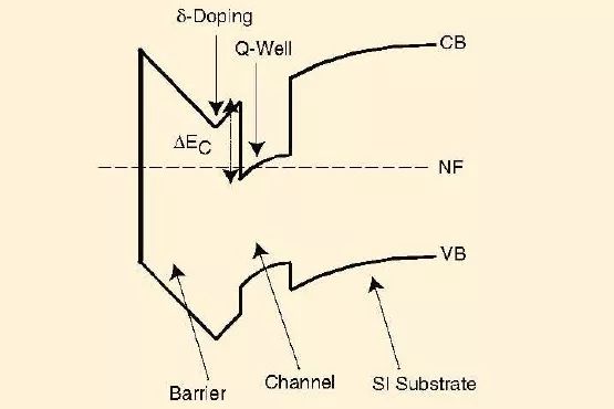
Figure 1. The energy band diagram of the HEMT heterostructure shows the narrow energy gap channel sandwiched between the semi-insulating (SI) substrate and the barrier layer. In this figure, the barrier layer is delta doped, which means the introduction of donor impurities into an extremely thin layer. The electrons in the channel accumulate in the quantum hydrazine at the interface, and the conduction band offset (ΔEc) of the interface controls the surface density ns.
Since the advent of HEMT technology, many improvements have been introduced to improve performance (ns and Vsate). The two main approaches are: 1) increase the conduction band shift, so as to accumulate more electrons in the interface quantum hydrazine, and 2) increase the mobility of the channel. In fact, this means increasing the In composition of the InGaAs channel. Content (from Xin=0% in conventional GaAsHEMT to Xin=80% in the highest speed InP HEMT).
Currently, two types of HEMT are being developed on GaAs substrates:
1) Mainstream GaAs P-HEMT (pseudomorphic HEMT) with an AlGaAs barrier layer and a stressed InGaAs channel is mainly used in low noise or power applications in the frequency range of 20-70 GHz [11]. 2) The use of GaAs M-HEMT (modified HEMT) can achieve higher speed, which is basically a lattice-matched InP structure (with an ALInAs/InGaAs heterojunction) grown on the relaxed buffer layer of the GaAs substrate structure). This structure benefits from the higher speed of InP-based structures and the low cost associated with larger, more brittle GaAs substrates. Although the thermal conductivity of the buffer layer is quite poor, this technology still shows excellent power and noise performance at 100 GHz.
In terms of maximum operating speed and higher output power, these performance records are still created by InP PM-HEMT, which exceeds 400mW at 90GHz and exceeds 2mW at 300GHz [14].
InP HBT
Together with the first report on the successful fabrication of a device using a material system that matches the InP substrate lattice, in the late 1990s, work on InP heterojunction bipolar transistors (HBT) officially entered the track[15] . This material system has several advantages over SiGe and GaAs, including:
1) InGaAs (lattice matched with InP) material has higher mobility and electron velocity than GaAs or SiGe. 2) Compared with GaAs, it has a lower surface recombination rate and thus a higher current gain, resulting in its ability to scale down to a smaller size. 3) Since the narrow band gap InGaAs is used in the base, it has a lower base-emitter turn-on voltage than GaAs. 4) When InP is used as a collector material, it has a higher breakdown electric field strength than SiGe. 5) The product has a higher breakdown electric field/cut-off frequency product than any other Si or III-V materials. 6) The maximum doping concentration of the InGaAs base and InGaAs emitter capping layer (Cap) is higher, resulting in lower parasitic contact resistance. 7) Since the crystal lattice of many trivalent semiconductor materials matches that of InP, it has an enhanced ability to "manipulate the energy gap" HBT.
Over the years, InP HBT has been responsible for the fastest benchmarking of transistor and circuit performance. Recently, the research groups in Santa Barbara and Illinois have reported on devices with Ft exceeding 700GHz and balanced devices with Ft/Fmax exceeding 500GHz [16], [17].
SiGe HBT-BiCMOS; CMOS and NMOS
The SiGe HBT developed in the late 1980s was produced using mature silicon technology. Through various developments, including the use of carbon doping and base self-aligned growth technology at the base, the device has achieved excellent performance-especially, the HBT in the Bi-CMOS configuration shows high Ft, Fmax (> 300GHz)[19]. In addition, the excellent 1/f noise performance, which is extremely useful in mixers and oscillators, is obtained due to a good passivation junction. All these characteristics have been used to make many operational chips, such as multiplexers (MUX) and demultiplexers (DEMUX), high-speed analog-to-digital converters in 43GHz optical fiber transmission systems [20], and The 77GHz frequency car radar chipset can even be used in transceivers operating above 100GHz [21].
In the past few years, with the adoption of the very short gate process (now in the 45-90nm range), people have reported n-channel MOS transistors with extremely high cutoff frequencies (ft>200GHz) [ twenty two]. This result, which is consistent with the semiconductor international technology development blueprint, is actually the result of the electron beam processing process that was previously limited to III-V HEMT (expensive) and the gate length reduction caused by many ongoing MOS structure evolutions. . Just like the HEMT structure, through the higher mobility channel (such as the acquired strained silicon channel) and the so-called high-K dielectric gate produced by the appropriate oxide thickness to channel length ratio, The performance has been enhanced (because SiO2 can provide unparalleled Si passivation, its relative dielectric constant-only 4-in the gate length, the gate thickness decreases proportionally, it becomes too low).
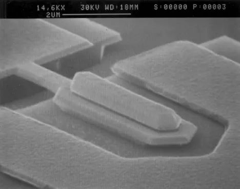
Figure 2. A photomicrograph of InP DHBT with an emitter width of 0.6μm before interconnection. HBT is made by using a triple-mesa self-aligning process [18].
Benefiting from this extended frequency performance, in the past few years, people have conducted a preliminary assessment of the potential of MOS technology in the millimeter wave field [23]. High integration and low cost (for a large number of chips) are the main reasons why we are interested in silicon technology.
III-V devices: co-integration with CMOS
In order to obtain the best advantages in both technical fields at the same time, the heterogeneous integration process is a promising solution. In order to closely integrate III-V transistors (actually InP transistors) and silicon-based CMOS, people have explored different approaches, especially in the COSMOS project funded by DARPA [24]. Several methods have been explored, from super self-aligned (less than 5μm) flip-chip integration to a completely complete monolithic mismatch epitaxial technology. The early results are very encouraging. After the InP device is integrated into the CMOS wafer, the performance degradation of the InP device is not obvious, and a class of large gain-bandwidth differential amplifier with large output swing and small power consumption has been demonstrated (>100GHz) [25]. Although there is no direct connection, people should pay attention to the progress made along the blueprint of the semiconductor international technology route through the study of the high-mobility III-V channel layer in MOSFET technology [26].
From transistor to circuit
In the previous section, we introduced the characteristics of existing different processes for active devices. These devices are the key to opening the door to frequencies above 100-GHz, but they are not enough. It also requires suitable ways to turn them into operable circuits, which means development in specific areas such as transmission lines, passive components, and grounding. Because of these factors, a certain process may be better than others when converting device characteristics to application areas.
At present, people can clarify that different technologies win in certain aspects, as shown in Table 3.
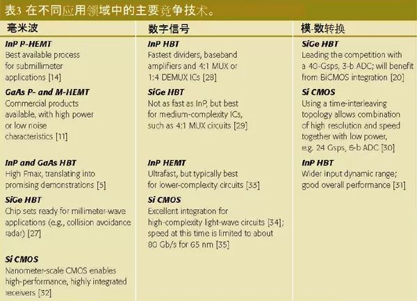
This table draws a picture of the current state of evolution. In the following discussion, two different types of demonstration circuits will be used to illustrate the screen in detail. T. Swan, Y. Baeyens, and M. Meghelli discussed the progress of specific 100-Gb/s lightwave circuits in this area [53].
Use static crossover as a benchmark for technology
The semiconductor process used in digital circuits is usually based on the performance of a static frequency divider. Since a static frequency divider uses flip-flop unit elements that can be found in more complex sequential circuits [36], the performance of such a circuit can be used as a recognized quality factor for digital integrated circuit technology. The same flip-flop is used as the frequency divider, the judgment circuit, and the basic unit of the 10/100-Gb/s system multiplexer [37]. In different circuits that use similar basic components, the reason for choosing a static divider is because it happens to be the easiest circuit for clear evaluation using simple measurement equipment, and it can give a clear upper limit on the performance that this technology can achieve .
Figure 3 shows the speed of static dividers reported from the early 1990s to the present. The data shows that in the past few years, even after the market for high-speed optical fibers collapsed in 2000, the speed has risen steadily. Most of the recent progress is funded by DARPA through the Frequency Agile Digital Synthetic Transmitter Technology (TFAST) program. Note that InP HBT technology continues to obtain the best results, with SiGe HBT following closely behind [38]. HEMT or CMOS device technology is not so competitive in terms of the highest frequency, because in FET-based devices, a large device size is required to meet the necessary transconductance requirements. So far, the best result of the static frequency divider published is the 150GHz achieved by 250-nm InP HBT technology. Recent progress has been focused on reducing power consumption [39]. This performance is consistent with the performance of the full-rate judgment circuit, and there is still much room for development in the performance of the multiplexer/demultiplexer (MUX/DEMUX) circuit.
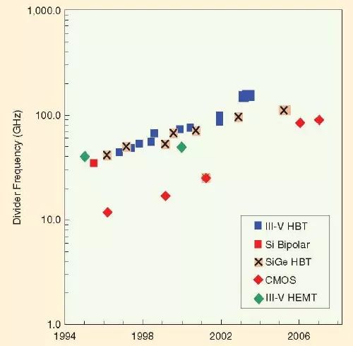
Figure 3. The maximum frequency of the static frequency divider changes with the reporting years. The data shown only contains the best results of the specific technology at the time.
At the highest operating speed, power consumption is particularly important, when a single gate circuit will consume several hundred milliwatts. Although the power consumption increases rapidly as the switching rate of the divider increases (for example, 23mW at 87GHz [41]), CMOS is added due to its excellent results (input frequency range is 90-100GHz [40]) Competition ranks. The best power consumption reported is using InP HBT technology, which is 42mW per latch at 150GHz [39].
Use oscillator (VCO) as a technical benchmark
Voltage Controlled Oscillator (VCO) is an indispensable building block for 100Gb/s serial transponders and millimeter wave communications, high-resolution radar and imaging systems. Such oscillators require a combination of low phase noise, high output power and good DC-to-RF conversion efficiency, especially at the highest frequencies. This translates into many important technical requirements.
• The highest oscillation frequency (fmax) is critical for sub-millimeter wave operation; the highest frequency fundamental frequency oscillator is based on nano-scale InP-based HEMT. The highest fundamental frequency oscillator reported is the 213-GHz InP HEMT oscillator with a history of ten years [42]. Recently, the use of 35-nm gate InP HEMT technology to further improve the fmax of devices with Fmax of 600-GHz enables the fundamental frequency oscillator to reach 346GHz[43]. InPDHBT also recently demonstrated fundamental oscillations at sub-millimeter wave frequencies [44].
• In order to obtain good close-in phase noise performance of the oscillator, it is important to use techniques with low flicker noise. Bipolar technologies such as SiGe or InP HBT can generally provide a lower 1/f corner frequency than FETs such as HEMT or CMOS, thanks to the reduction of surface state effects. When observing the phase noise at large frequency deviations (for example, 1MHz from the carrier-see Figure 4), the phase noise exhibited by the millimeter wave CMOS oscillators is close to that of their corresponding SiGe and InP HBT devices. This comparison does not take the influence of the tuning range into account, and it will be misinterpreted. As mentioned in [45], the oscillator millimeter-wave frequency phase noise will be better without output buffering.
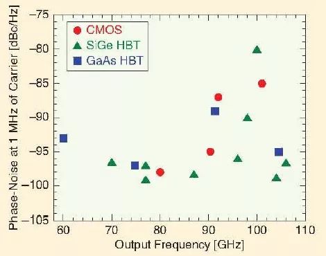
Figure 4. The reported phase noise overview of millimeter wave oscillators implemented with different technologies (at 1-MHz off the carrier).
• Finally, the achievable output power of the oscillator at the highest frequency has become an important design parameter, especially when the device is operating close to its fmax, because at this time it will become extremely difficult to further amplify the output signal . In order to maximize the output power, the internal voltage swing of the oscillator needs to be maximized. Most III-V devices, such as InP HBT, have an uncompromising advantage in terms of breakdown voltage, especially when compared to CMOS. This will produce the reported higher output power.
Push-push oscillator with high efficiency and high power source above 100GHz
In order to achieve higher oscillator output power above 100GHz, designers are more inclined to push-push the oscillator topology, in which the outputs of two oscillators coupled in opposite phases are combined to produce one Output signal with strong second-order harmonics. This topology makes it possible to achieve signal sources higher than fmax on the existing active device technology, and can extend the frequency range of the existing high-Q resonator technology [46]. In addition, with the push-push topology, a static or dynamic frequency divider that works at the fundamental frequency instead of the second-order harmonic output frequency can be used to lock the phase-locked loop (PLL) oscillator to achieve frequency-locked signal source , Thereby reducing the speed requirement of the frequency divider by half.
The potential of the millimeter wave frequency push-push oscillator has been fully demonstrated. Push-push oscillators implemented with different compound semiconductor technologies have been reported in the literature: in [47] reported 0.13μm GaAs PHEMT oscillators up to 140GHz, and reported in [48] up to 278GHz SiGe HBT oscillator. Even the use of CMOS technology has successfully achieved signal sources above 100 GHz: people have reported a 192 GHz push-push oscillator using 130-nm CMOS technology [49]. Recently, 45-nm CMOS technology was used to construct a signal source operating at 410 GHz [50]. However, even with the push-push topology, due to the reduced breakdown voltage of silicon-based high-speed technology and the need for nano-level CMOS to work at low bias voltages, it can be observed that the CMOS push-push oscillator is significantly reduced above 100GHz The output power. For example, a 410-GHz CMOS signal source has an output power of 20nW, which may not be sufficient for use in transmitter applications or to drive mixers in receivers. As explained in the following paragraphs, the ideal choice for a push-push oscillator with such high power is the InP double-heterojunction HBT (D-HBT) technology, which combines high fmax and high breakdown voltage. together.
The integrated push-push oscillator with oscillation frequency at 220 and 355GHz is realized by Alcatel-Lucent/Bell-Lab's 0.5μm emitter InGaAs/InP HBT D-HBT technology, with a maximum oscillation frequency of 335GHz and 4V Breakdown voltage (Vbceo) [51].
These oscillators are based on a balanced Colpitts oscillator topology. By synthesizing the outputs with opposite phases, and using short stubs to adjust the oscillator output impedance at the second-order harmonic frequency through the reactance part to generate a strong second-order harmonic signal [52], such as As shown in Figure 5. People have implemented different resonators using this technology. Figure 5 shows a 287GHz circuit layout. The transmission line resonators LE, LB and LC are realized by thin-film microstrip lines on a 7-μm low-K interlayer dielectric material (εr=2.6) using a 2-μm thick gold plate ground plane.
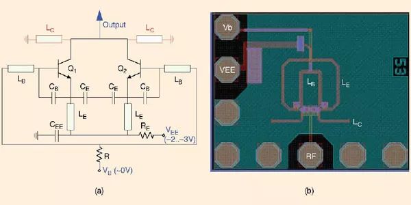
Figure 5. (a) circuit diagram and (b) circuit layout diagram of an InP D-HBT push-push oscillator [52].
The output signals of different oscillators are detected by a WR03 waveguide probe and down-converted using a WR03 sub-harmonic mixer. The measured output power at 210GHz and 235GHz can reach 1mW, and the DC-to-RF efficiency is 2-3%. Oscillators operating at 280 and 297GHz can obtain -5dBm output power. Figure 6 shows the measured output spectrum of the highest frequency oscillator implemented. Although the output exceeds the frequency range of the WR03 waveguide (LO) on-chip probe and down-conversion mixer, when the oscillator signal is mixed with the effective local frequency of 321.6GHz, a strong IF signal will still be detected. By correcting the loss of the probe and mixer, the loss value is estimated to be between 23dB and 30dB, and the output power higher than -13dBm can be obtained at 355GHz.
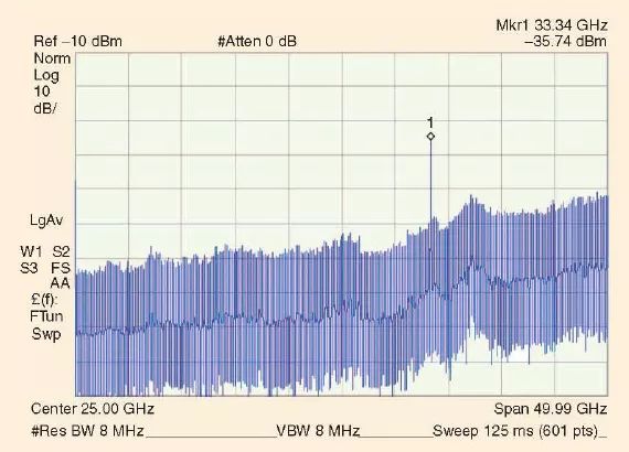
Figure 6. The downconversion spectrum of an InP D-HBT push-push VCO operating at 355GHz (LO=321.6GHz, upper sideband) (without any correction for the loss of the mixer).
The relationship between the output power of these oscillators and the oscillation frequency is shown in Figure 7, and compared with oscillators made by different semiconductor technologies. Thanks to the high breakdown voltage of InP D-HBT and the second-order harmonic tuning technology that can improve the output power by 5dB, up to now, the InP D-HBT push-push oscillator can have better performance in this frequency range than reported Other transistor signal sources have higher output power and efficiency.
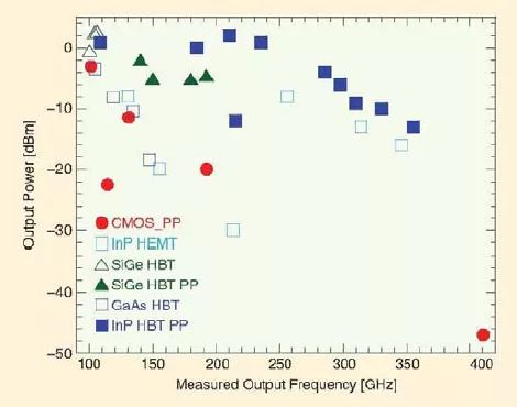
Figure 7. The reported overview of the output power and operating frequency of oscillators implemented with different technologies. The results of using the fundamental frequency and push-push oscillators are represented by hollow and solid symbols, respectively.
in conclusion
Several semiconductor materials and technologies are suitable for solving 100GHz and 100-Gb/s application problems. These technologies sometimes compete with each other. As we expected, this is a new application field, and people are still discussing the advantages and disadvantages of these technologies. This article aims to illustrate the diversity of these evolving technologies and their potential impact as frequency performance continues to improve. Although for a long time, the improvement of device performance only depends on the size reduction allowed by the advancement of lithography technology, but the heterostructure and stress engineering technology have now become powerful means through which they can enhance the speed and power performance. Reach the level that can open the door to 100-GHz and 100-Gb/s application areas.
RF Connector Adapter,RF Adapters SMB To SMC,RF Adapters N To BNC,Plug To Plug Adapter Connectgor
Xi'an KNT Scien-tech Co., Ltd , https://www.honorconnector.com