When designing a switching power supply, you may have heard of electromagnetic interference (EMI)
More and more applications must pass EMI standards before manufacturers can obtain commercial resale approval. Switching power supply means that there are electronic switches inside the device through which EMI can generate radiation.
This article will introduce the sources of EMI in switching power supplies and methods or techniques to reduce EMI. This article will also show you how the power module (controller, high-side and low-side FET and inductor package in one package) can help reduce EMI.
The source of EMI in switching power supply
First of all, the laws of physics must be respected. According to Maxwell's equations, alternating current can generate electromagnetic fields. This phenomenon occurs in every electrical conductor, which itself has some capacitance and inductance that can form an oscillating circuit. The oscillating circuit radiates electromagnetic energy into space at a specific frequency (f=1/(2*Ï€*sqrt(LC))). This circuit acts as a transmitter of electromagnetic energy, but it can also receive electromagnetic energy and act as a receiver. The antenna design is to maximize the transmitted or received energy.
But not every application should be like an antenna, and this design may have negative effects. For example, switching step-down power supplies are designed to convert higher voltages to lower voltages, but they also act as (harmful) electromagnetic wave transmitters, which may interfere with other applications, such as the AM frequency band. This effect is called EMI.
In order to ensure the normal operation of functions, it is very important to minimize EMI sources. The International Special Committee on Radio Interference (CISPR) has defined various standards, such as CISPR 25 as a benchmark for automotive electrical applications, and CISPR 22 for information technology equipment.
How to reduce the EMI radiation of the power supply design? One method is to completely shield the switching power supply with metal. But in most applications, this method cannot be implemented due to cost and space reasons. A better method is to reduce and optimize EMI sources. Many literatures have discussed this topic in detail; this article recommends two approaches.
Let us review the main sources of EMI in switching power supplies and why power modules can help you easily reduce EMI.
Reduce the current loop in the layout
As the name implies, the switching power supply is used for conversion. Their function is to turn on and off the input voltage at a frequency of several hundred kilohertz to several megahertz. This leads to fast current conversion (dI/dt) and fast voltage conversion (dV/dt). According to Maxwell's equations, alternating current and voltage produce alternating electromagnetic fields. These electromagnetic fields diffuse radially from their origin, and their intensity decreases with distance.
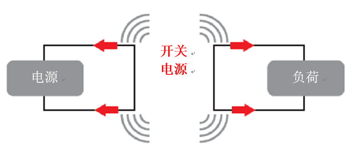
Figure 1. EMI from a switching power supply will affect the load and the main power supply.
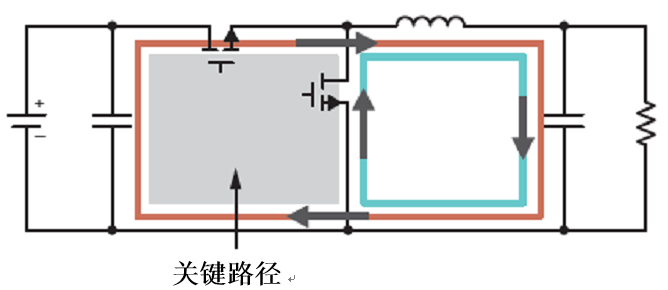
Figure 2. A critical current loop is formed between the input, switch, and input capacitor.
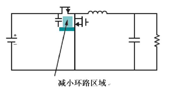
Figure 3. Reducing the loop area helps reduce EMI
Magnetic and electric fields can interfere with the conductive parts of the application (for example, copper traces on a printed circuit board [PCB], like an antenna) and generate additional noise on the line, which in turn can cause EMI (see Figure 1). In fact, the conversion of a few watts of power will expand the range of EMI radiation.
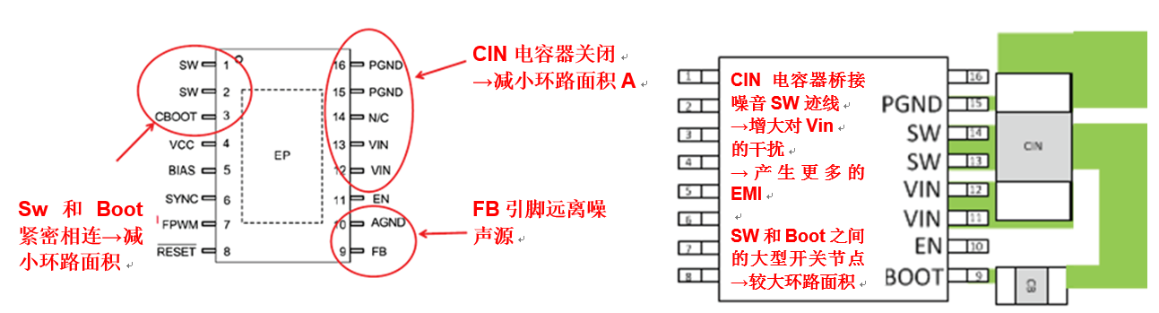
Figure 4. Pin arrangement helps reduce loop area. Left picture: optimized pin arrangement; right picture: non-optimized layout, it is almost impossible to form a good layout.
The radiated electromagnetic energy is proportional to the amount of current (I) and loop area (A) flowing through it. Reducing the area of ​​AC current and voltage loops helps reduce EMI (see Figure 2 and Figure 3).
Focusing on the pin layout (see Figure 4) can help you design a better layout by reducing the area of ​​the high dI/dt loop. For example, switching nodes can cause high current changes (dI) and high voltage transitions (dV). A good pin arrangement can separate noise-sensitive pins and noise pins. The switch node and start pin should be as far away as possible from the noise-sensitive feedback pin. In addition, the input pin and the ground pin should be adjacent. This simplifies the wiring on the PCB and the placement of the input capacitor.
Figure 5 shows the improved evaluation module (EVM) of the LMR23630 SIMPLE SWITCHER® converter. The two input capacitors are about 2.5 cm away from the input pins. The reason for this arrangement is to simulate a poor layout, because the current loop area (the red rectangle in Figure 5) is larger than the data sheet requires and recommends. The elliptical red shape in Figure 5 represents the switching node between the converter and the inductor. The loop area between the IC and the inductor is as small as possible.
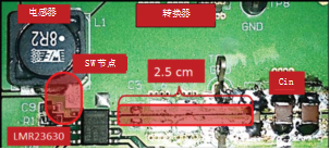
Figure 5. An example of an incorrect layout with a large loop area (red rectangle) between the input pin and the input capacitor. A second loop area (elliptical red shape) is formed between the IC and the inductor.
The graph in Figure 6 shows the EMI radiation of the LMR23630 converter, where only the loop area formed between VIN, GND and the input capacitor is different. In a good layout, the capacitor is as close as possible to the input pin and ground pin (the loop area is as small as possible). In a poor layout, the input capacitor is 2.5 cm away from the input pin, thus forming a larger loop area.
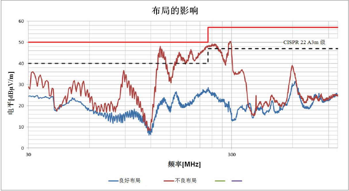
Figure 6. The effect of the layout of the input capacitor of the LMR23630 converter on EMI radiation.
The red line of the graph in Figure 6 represents the EMI radiation of a poor layout. The blue line represents the EMI radiation of a good layout with the same EVM. Modifying the area of ​​a loop can have a huge impact. The EMI radiation level of the LMR23630 converter can be reduced by more than 20 dBμV/m.
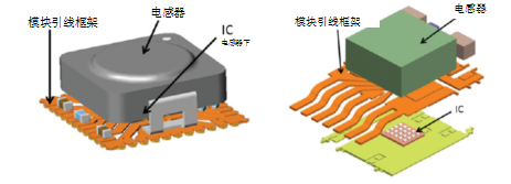
Figure 7. The internal composition of different types of power modules. In both cases, the inductor is located on the top of the IC die.
Therefore, when designing with a step-down converter or a step-down power module, how to place the input capacitor should be one of the first considerations. The power module also has the following advantages: The critical loop area between the inductor and the IC has been optimized. The inductor is connected to the integrated circuit inside the package (see Figure 7). This placement will form a smaller loop area inside the package. Therefore, it is not necessary to wire the noise switch node on the printed circuit board.
Most of the inductors are shielded in the power module to prevent electromagnetic radiation from the coil. High current-to-voltage conversion occurs very close to the inductor, and a part of the electromagnetic field of the switch node is shielded, and the inductor is located on the top of the lead frame (see Figure 7).
Fast voltage and current transients
Fast transients can cause ringing at the switching node, which can cause EMI. In some cases, the converter can be connected to the start pin. Placing a resistor in series with the starting capacitor will increase the rise time (dt), reducing efficiency while reducing EMI.
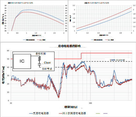
Figure 8. The effect of adding a startup resistor to the switch node of the LMR23630 converter. EMI radiation is low, but due to high switching losses, efficiency is reduced.
Figure 8 shows the EMI emission scan of the LMR23630 EVM. After changing the layout, place the input capacitor about 2.5 cm away from the pin to simulate a bad layout and show how the placement of the starting capacitor will affect the EMI characteristics. It may be easier to put an extra startup capacitor in the design than to completely change the layout. It is recommended that you always take the starting capacitor into consideration when designing, in case you need it from time to time. If not, you can use 0Ω resistors to reduce the space on the PCB.
Putting the starting resistor in series with the starting capacitor can reduce the EMI spectrum. Emissions in certain frequency ranges can be reduced by up to 6dB. Figure 8 also shows the efficiency balance. Using a 30.1Ω resistor to shorten the rise time dt reduces the efficiency by more than 1%.
Look at the power loss to illustrate this point even more. The power loss at full load (3A) is increased from 1.9W to 2.1W. When the power loss exceeds 10%, it may cause heat dissipation problems.
Placing a small Schottky diode between the switch node pin and the ground pin can reduce the reverse recovery current, thereby reducing the switch node current ringing dI in the synchronous converter, but this will increase the bill of materials (BOM) cost. Alternatively, you can add a snubber network that contains an extra large package capacitance and resistance between the switch node and ground. The buffer can consume the energy of the switch node's ringing, but it needs to know the ringing frequency of the additional components and calculate it correctly. This method will also reduce the efficiency of the switching power supply.
Parasitic inductance and capacitance in the current path
For a synchronous buck converter, each IC architecture will generate noise of different intensities, which is manifested as EMI radiation. But it is difficult to find this item from the data sheet. Most data sheets do not provide EMI diagrams, because PCB layout, BOM components and other factors will have an impact on EMI characteristics. If you are lucky, the EVM user guide will provide an EMI characteristic diagram for this particular design. But if your design does not match the layout and BOM of the EVM, the EMI characteristics of the application you are designing may be very different. The power module simplifies the layout and realizes a quick and easy design, because you only need to consider some rules of thumb. For example, minimize the number of traces or cuts in the ground plane; if necessary, design them to be parallel to the current direction (Figure 9).
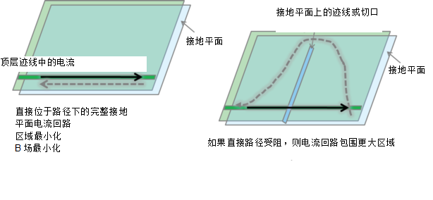
Figure 9. Cutouts and traces in the PCB affect the current and therefore also affect the radiated EMI.
Protect noise-sensitive nodes from the influence of noise nodes
Shorten the noise-sensitive nodes as much as possible and keep them away from the noise nodes. For example, the long trace from the resistor divider network to the feedback (FB) pin can act as an antenna and capture noise from electromagnetic radiation (Figure 10). This noise will be introduced into the FB pin, causing additional noise at the output, and even making the device unstable. It is a challenge to take all of this into consideration when designing the layout of the switching buck regulator.

Table 1. Examples of noise-sensitive nodes and noise nodes in a buck converter.
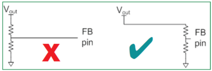
Figure 10. Always place the resistor divider on the FB pin as close to the FB pin as possible.
The advantage of the module is to keep noise-sensitive nodes and noise nodes to a minimum, thereby minimizing the chance of incorrect layout. The only thing to note is to keep the trace of the FB pin as short as possible.
in conclusion
There are many knobs used to adjust EMI in switching buck converters, but it may not be convenient to implement the best solution. Finding the best configuration takes a lot of valuable design time. Power modules already include FETs and inductors, which makes it simple and fast to create and complete a power supply design with good EMI characteristics. The most critical point when designing with a step-down module is the placement of some external components, which helps to significantly improve EMI characteristics.
EMI comparison of converters and power modules
The previous article explained the source of EMI in switching power supplies and how to reduce EMI. Now, this article will demonstrate how the module can help reduce EMI emissions by comparing the measurement results between a converter and a power module using the same integrated circuit (IC). Both are from TI’s SIMPLE SWITCHER product line, the converter is LMR23630, the power module is LMZM33603, and the LMR23630 IC is used. Partial changes are made to the EVM of the two devices to obtain the same BOM number, so the result depends only on the selected component (converter or power module) and layout. Both EVMs have a good optimized layout. After that, placing the capacitor far away from the input pin creates a bad layout.
LMR23630 converter performance
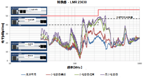
Figure 11. EMI emissions of LMR23630 converters with different input capacitor layouts.
Figure 11 shows four different EMI spectrums for different design layouts. The design layout is arranged from best to worst (similar to Figure 5, but separates the steps). In the first measurement (good layout/blue line), no changes were made to the layout of the EVM (all input capacitors in a good layout are very close to the input pins). In the second measurement (small capacitor near/red line), two 4.7μF capacitors are placed 2.5 cm away from the input pin. The small 0.22μF capacitor is very close to the input pin. In the third (small capacitor away from/green wire) and fourth (no small capacitor/purple wire) measurements, the small capacitor is 2.5 cm away from the input pin, and then completely removed.
You can see in Figure 11 that the placement of the input capacitor is critical. Placing the small input capacitor away from the input pin or removing it completely would violate the CISPR 22 A3M standard. Placing small capacitors close to the input pins can minimize the high-frequency loop area. Small capacitors can filter out high-frequency noise, while capacitors with larger capacitance can filter out low-frequency noise.
A small input capacitor is usually included in the package of the power module. Let us look at the performance of the power module when the layout is poor.
Performance of LMZM33603 power supply module
Figure 12 shows the EVM layout of the power modules, also arranged from best to worst. The blue line represents the EMI radiation of the unchanged EVM. The red and green lines indicate poor layout. One of the lines has two 4.7μF input capacitors located under the bottom of the PCB (red line). The capacitor on the green line is about 3.5 cm away from the input pin (highlighted by a red oval in Figure 13). The thick red line in Figure 13 also shows the modified EVM and the critical loop area formed between VIN, input capacitor, and ground. The EMI characteristics deteriorate, but it does not violate the CISPR 22 A3M level standard.
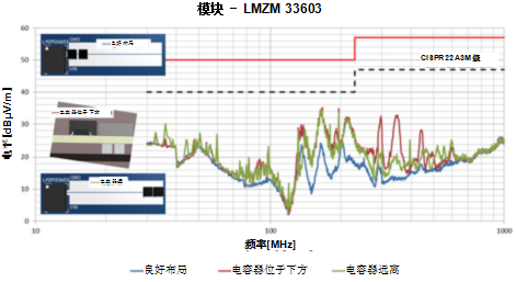
Figure 12. EMI radiation characteristics of TI LMZM33603 power module
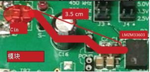
Figure 13. Example of poor layout of TI LMZM33603 power module.
Power modules can remedy layout design errors
Figure 14 compares the LMR23630 converter (red line) and the LMZM33603 power module (blue line) in a single chart. Both have similar bad layouts, and all external input capacitors are kept away from the input pins.
Obviously, the EMI radiation characteristics of the LMZM33603 power module are better than those of the LMR23630 converter. Although the two layouts are not perfect, the power module will pass the CISPR test, and the converter will not pass the test.
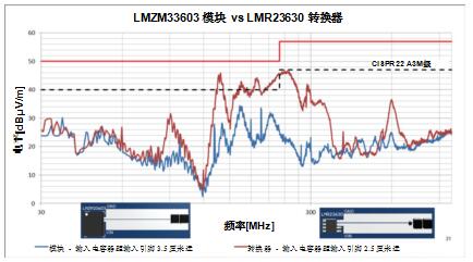
Figure 14. Compare the EMI characteristics of TI LMR23630 converter and LMZM33603 power module.
in conclusion
As mentioned earlier, it is challenging to create a good layout design for a switching power supply. Even experienced engineers can easily make mistakes, such as improper placement of input capacitors.
The power module is more conducive to reducing design layout errors. In terms of meeting EMI characteristics, they are ideal for switching power supplies and are essential for efficient use of design time.
To read other articles on creating a good layout to reduce EMI, please check the application report, "AN-2155 Layout Tips for EMI Reduction in DC/DC Converters" and "AN-643 EMI/RFI Board Design".
Nano atomization, the desktop will not be wet when humidified, and the water molecules are refined into fine particles, which are more easily absorbed by the skin. Touch button operation, press once to continuously emit fog, press twice to intermittently emit fog, different modes have different experiences. Intelligent power-off design, automatic power-off protection for water shortage, prevent dry burning, and use more assured.
Home Humidifier,Air Evaporative Humidifier,Home Ultrasonic Air Humidifier,Portable Whole House Humidifier
Dongguan Yuhua Electronic Plastic Technology Co.,Ltd , https://www.yuhuaportablefan.com