TI's TDA2x is a system-on-chip (SoC) that meets the requirements of Advanced Driver Assistance Systems (ADAS) design, using a multi-phase scalable architecture that includes fixed and floating point TMS320C66x digital signal processor (DSP) to generate cores, Vision AcceleraTIonPac, ARMCortex-A15 MPCoreTM and dual Cortex-M4 processors. Also integrated with main peripherals, including multi-camera interface (parallel and serial) for LVDS surround systems, display, CAN and GigB Ethernet AVB. Main Used in single or stereo front-end cameras, LVDS or Ethernet look-around and sensor fusion such as visual, radar, ultrasonic and lidar sensors. This article describes the main features of the TDA2x series, block diagrams and evaluation modules TDA2x EVM including TDA2x EVM CPU board and VisionSuper28 video Application board main features, circuit diagrams and bill of materials.
TI's new TDA2x System-on-Chip (SoC) is a highly opTImized and scalable family of devices designed tomeet the requirements of leading Advanced Driver Assistance Systems (ADAS). The TDA2x familyenables broad ADAS applications in today's automobile by integrating an optimal mix of performance , lowpower and ADAS vision analytics processing that aims to facilitate a more autonomous and collision-freedriving experience.
The TDA2x SoC enables sophisticated embedded vision technology in today's automobile by enabling theindustry's broadest range of ADAS applications including front camera, park assist, surround view andsensor fusion on a single architecture.
The TDA2x SoC incorporates a heterogeneous, scalable architecture that includes a mix of TI's fixed and floating-point TMS320C66x digital signal processor (DSP) generation cores, Vision AccelerationPac, ARMCortex-A15 MPCoreTM and dual-Cortex-M4 processors. The integration of a video Efficient for decoding multiple video streams over an Ethernet AVB network, along with graphics accelerators for renderingvirtual views, enable a 3D viewing experience. And the TDA2x SoC also integrates a host of peripherals including multi-camera interfaces (both parallel and serial) for LVDS-based surround View systems,displays, CAN and GigB Ethernet AVB.
The Vision AccelerationPac for this family of products includes multiple embedded vision engines (EVEs)offloading the vision analytics functionality from the application processor while also reducing the powerfootprint. The Vision AccelerationPac is optimized for vision processing with a 32-bit RISC core for efficient program execution and a vector coprocessor for specialized vision processing.
Additionally, TI provides a complete set of development tools for the ARM, DSP, and EVE coprocessor, including C compilers, a DSP assembly optimizer to simplify programming and scheduling, and adebugging interface for visibility into source code execution. The TDA2x ADAS processor is qualified According to the AEC-Q100 standard.
Main features of TDA2x series: 1
• Architecture Designed for ADAS Applications
• Video, Image, and Graphics Processing Support
– Full-HD Video (1920 × 1080p, 60 fps)
– Multiple Video Input and Video Output
• ARM® Dual Cortex®-A15 MicroprocessorSubsystem
• Up to Two C66xTM Floating-Point VLIW DSP
– Fully Object-Code Compatible With C67xTM and C64x+TM
– Up to Thirty-two 16 × 16-Bit Fixed-PointMultiplies per Cycle
• Up to 2.5MB of On-Chip L3 RAM
• Level 3 (L3) and Level 4 (L4) Interconnects
• Two DDR2/DDR3/DDR3L Memory Interface (EMIF) Modules
– Supports up to DDR2-800 and DDR3-1066
– Up to 2GB Supported per EMIF
• Two ARM® Dual Cortex®-M4 Image ProcessingUnits (IPUs)
• Vision AccelerationPac
– Up to Four Embedded Vision Engines (EVEs)
• IVA-HD Subsystem
• Display Subsystem
– Display Controller With DMA Engine and up toThree Pipelines
– HDMITM Encoder: HDMI 1.4a and DVI 1.0Compliant
• 2D-Graphics Accelerator (BB2D) Subsystem
– VivanteTM GC320 Core
• Video Processing Engine (VPE)
• Dual-Core PowerVR® SGX544TM 3D GPU
• Three Video Input Port (VIP) Modules
– Support for up to 10 Multiplexed Input Ports
• General-Purpose Memory Controller (GPMC)
• Enhanced Direct Memory Access (EDMA) Controller
• 2-Port Gigabit Ethernet (GMAC)
• Dual Controller Area Network (DCAN) Modules
– CAN 2.0B Protocol
• PCI-Express® 2.0 Port With Integrated PHY
– One 2-lane Gen2-Compliant Port
– or Two 1-lane Gen2-Compliant Ports
• Sixteen 32-Bit General-Purpose Timers
• 32-Bit MPU Watchdog Timer
• Ten Configurable UART/IrDA/CIR Modules
• Four Multichannel Serial Peripheral Interfaces (MCSPIs)
• Quad SPI Interface
• Five Inter-Integrated Circuit (I2C) Ports
• SATA Interface
• Multichannel Audio Serial Port (MCASP)
• SuperSpeed ​​USB 3.0 Dual-Role Device
• Up to 247 General-Purpose I/O (GPIO) Pins
• Real-Time Clock Subsystem (RTCSS)
• Devise security features
– Hardware Crypto accelerators and DMA
– Firewalls
– JTAG lock
– Secure keys
– Secure ROM and boot
• Power, Reset, and Clock Management
• On-Chip Debug With CTools Technology
• Automotive AEC-Q100 Qualified
• 28-nm CMOS Technology
• 23 mm × 23 mm, 0.8-mm Pitch, 760-Pin BGA (ABC)
TDA2x series applications:
• Mono or Stereo Front Camera
– Object Detection
– Pedestrian Detection
– Traffic Sign Recognition
– Lane Detection and Departure Warning
– Automatic Emergency Braking
– Adaptive Cruise Control
– Forward Collision Warning
– High Beam Assist
• LVDS or Ethernet Surround View
– 3D surround view
– Rear object detection
– Parking assist
– Pedestrian Detection
– Lane tracking
– Drive Recording
• Sensor Fusion – Vision, Radar, Ultrasonic, Lidarsensors
– Object data fusion
– Raw data fusion
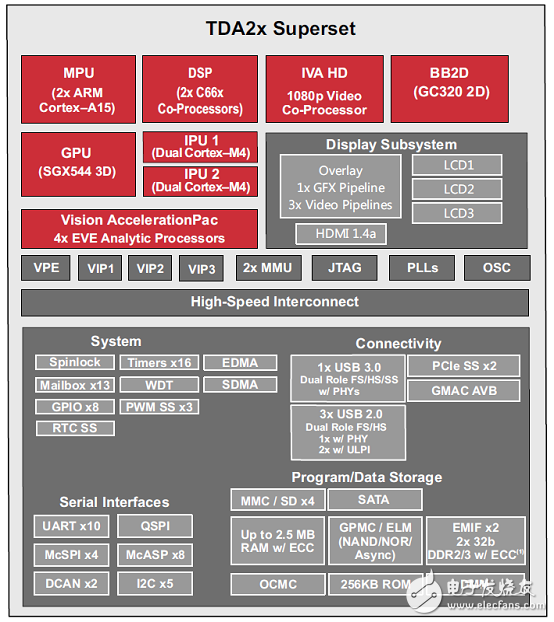
Figure 1. TDA2x Series Block Diagram
Evaluation Module TDA2x EVM
TDA2x EVM is an evaluation platform designed to speed up development efforts and reduce time to market for ADAS applications. It is based on TDA2x SoC which incorporate a heterogeneous, scalable architecture that includes a mix of TI's fixed and floating-point TMS320C66x digital signal processor ( DSP) generation cores, Vision AccelerationPac (EVE), ARM Cortex-A15 MP CoreTM and dual-Cortex-M4 processors. Also it integrates a host of peripherals including multi-camera interfaces (both parallel and serial) for LVDS-based surround view Systems, displays, CAN and GigB Ethernet AVB.
The main board integrates these key peripherals such as Ethernet, FPD-Link and HDMI, while the Vision application board provides interfaces for popular imagers.
Please note that a power supply is NOT included with the TDA2x Evaluation Module and needs to be purchased separately. A power supply with the following specs is needed:
12V DC output
5A output
Positive inner and negative outer terminals
Female barrel with 2.5mm or 2.1mm inner diameter and 5.5mm outer diameter, insertion depth is 8.85mm
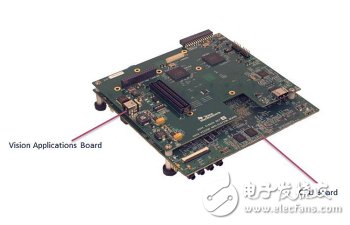
Figure 2. Outline of the evaluation module TDA2x EVM5777G-03-40-00
1.TDA2x EVM CPU board
The TDA2x EVM is an evaluation platform designed to speed up development efforts and reduce time to market for ADAS applications. The TDA2x EVM is based on TDA2x System-on-Chip that incorporate aheterogeneous, scalable architecture that includes a mix of TI's fixed and floating-point TMS320C66xdigital signal processor (DSP) generation cores, Vision AccelerationPac (EVE), ARM® Cortex®-A15 MPCore and dual-Cortex-M4 processors. Also it integrates a host of peripherals including multi-camerainterfaces (both parallel and serial) for LVDS- Based surround view systems, displays, CAN and GigBEthernet AVB.
The main CPU board integrates these key peripherals such as Ethernet or HDMI, while the vision application daughter board and LCD/TS daughter board will complement the CPU board to deliver complete system to jump start your evaluation and application development.
An EVM system is comprised of a CPU board with one or more application board(s). The CPU boardcan be used standalone for software debug and development. Each EVM system hasbeen designed to enable customers to evaluate the Processor performance and flexibility in the following targeted markets:
• Automotive Infotainment applications
• Automotive Vision applications
• Emerging End Equipment applications
The CPU board contains the (Jacinto 6/TDA2x) applications processor, a companion Power ManagementIC (TPS659039), Audio Codec (TLV320AIC3106), DDR3 DRAM, four different Flash memories (QSPI, eMMC, NAND and NOR), a multitude of interface ports And expansion connectors. The board provides additional support components that provide software debugging, signal routing and configuration controls that would not be needed in a final product. Different version CPU boards will be built to support the development process that include:
• Socketed processor used for wakeup, early software development, quick and easy signal revisionevaluation
• Soldered-down processor used for high performance Use Cases and evaluations
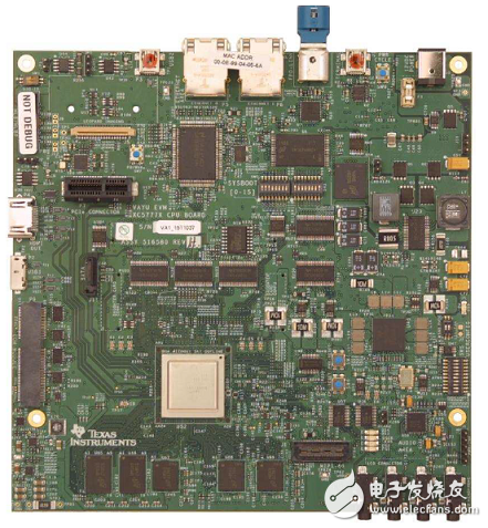
Figure 3. Outline of the TDA2x EVM CPU board
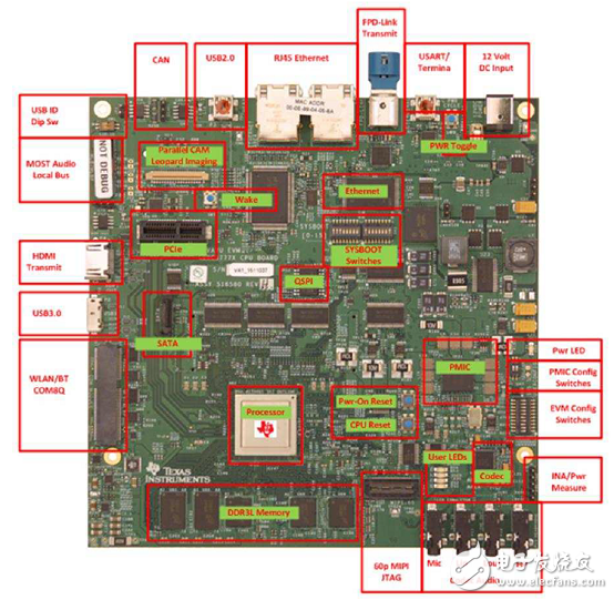
Figure 4. Distribution of main components of the TDA2x EVM CPU board
Key features of the TDA2x EVM CPU board:
• Processor:
– SoC (23mm x 23mm package, 0.8mm pitch with 28x28 via-channel array)
– Support for corresponding socket
• Memory:
– EMIF1 - DDR3L-1066 (with ECC): two 8Gbit (16bit data/ea) and one 4Gbit (8bit data, for ECC) memory devices
– EMIF2 - DDR3L-1066: four 4Gbit (8bit data/ea) memory devices
– QSPI (Quad SPI)
– eMMC
– NAND flash memory 16 bit
– NOR flash memory
– I2C EEPROM
• Boot mode selection DIP switch
• On-Board Temperature Sensor
– TMP102
• JTAG/Emulator:
– 60-pin MIPI Connector
– 20-pin-CTI adapter: 10 x 2, 1.27mm pitch
– 14-pin adapter: 7 x 2, 2.54mm pitch
• Audio input and output:
– AIC3106 codec: Headphone OUT, Line OUT, Line IN, Microphone IN
• Connectors and Transceivers:
– CAN Interface - 2-wire PHY on DCAN1
– Two USB Host receptacles:
• USB3.0 (micro-USB)
• USB2.0 (mini-USB)
– PCIe x 1
– Video - one HDMI Out, one FPD-Link III, one LCD
– MLB and MLBP on Mictor connector
– RS232 via USB FTDI converter (mini-A/B USB)
– COM8 connector
– Gigabit Ethernet PHY (RJ45) x 2
– MicroSD socket
– SATA
– I2C Expander
– LCD Daughter Board connector
• Power supply:
– 12 V DC input (Wall supply not supplied with Kit)
– Optimized Power Management IC (PMIC) Solution
– Support sleep mode with wake-up capability
• PCB:
– Dimension (W x D): 170mm x 170mm
– Expansion Connectors to support application boards
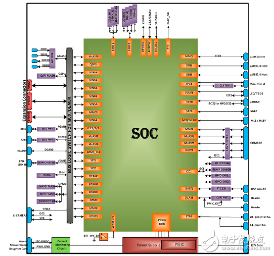
Figure 5. Functional Block Diagram of the TDA2x EVM CPU Board
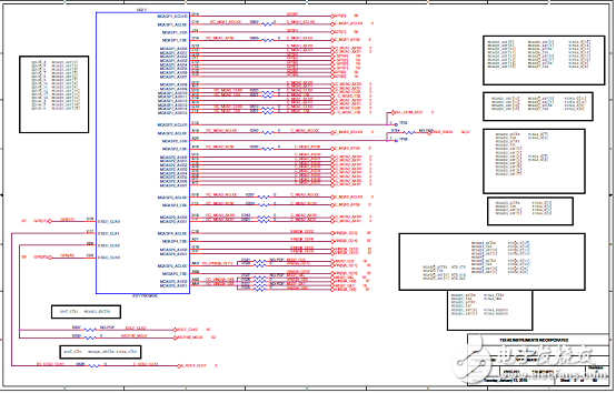
Figure 6. TDA2x EVM CPU Board Circuit Diagram (1)
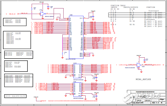
Figure 7. TDA2x EVM CPU Board Circuit Diagram (2)
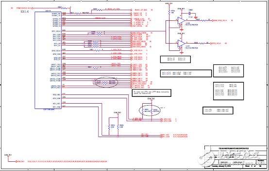
Figure 8. TDA2x EVM CPU Board Circuit Diagram (3)
For the remaining 80 circuit diagrams see: sprr210
2.VisionSuper28 video application board
The vision application board supports automotive vision video multiplexing options for different video inputsources. As the board supports multiple video inputs and multiplexing options, it is a solution for advanced driver assistance systems (ADAS) development activity. This evaluation module (EVM) is based on TIVisionSuper28 -series System-on-Chip (SoC) silicon solutions.
The vision application, based on the VisionSuper28 EVM, consists of the following:
• Application board
– Supports the multiplexing option for proprietary camera modules
– Supports FPD-Link III FMC DS90UB914Q daughter board for stereoscopic view and/or surroundview camera interface
– Supports HDMI and CAN interfaces
• FPD-Link III FMC DS90UB914Q daughter board
– Supports four high-resolution cameras for surround view
– Supports five or six lower-resolution cameras for surround and stereoscopic view
• VisionSuper28 CPU board
– Supports SoC
– Supports memory devices, other interfaces, and so forth
• Stand-alone camera module head boards
– AR0132AT6C00XPEAH-E head board from AptinaTM
– OV10635 head board from OmniVisionTM
– Single-imager head board from Leopard imaging
– LI-M024-DUAL image head board from Leopard imaging (LI)
• Four surround-view image sensor head boards with serializer boards
• Stereoscopic-view image sensor head boards with serializer boards
• Linear guide rail to adjust the position of stereoscopic image sensor
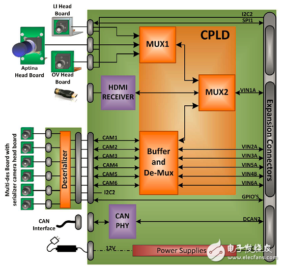
Figure 9. Block diagram of the VisionSuper28 video application board
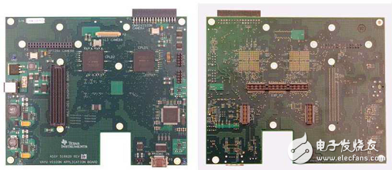
Figure 10. Outline of the VisionSuper28 Video Application Board
Left: top view right: bottom view
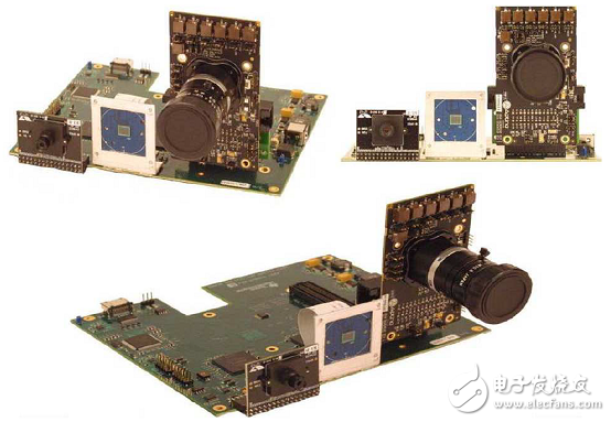
Figure 11. VisionSuper28 video application board and image header connection diagram
Main features of the VisionSuper28 video application board:
• Power supply
– 12-V DC input
– Power-on cycle sync-up with CPU board
• PCB
– Dimension (W × D): 170 mm × 140 mm
– Supports a multi-des card for surrounding view
• CPLD
– Multiplexing
– De-multiplexing
– Buffer
– Skew matching
– Control and status indication
• HDMI receiver – ADV7611 (Rev C and earlier use SiI9127)
• CAN transceiver
• Image sensors interface
– Aptina image sensor
– LI image sensor head boards with Aptina and OmniVision sensors
– OmniVision image sensor
• FPD-Link III FMC DS90UB914Q daughter board
– For stereoscopic view
– For surrounding view
• Linear guide rail
– For adjusting the stereoscopic view
• Connectors and headers
– CAN interface header
– HDMI receiver connecter
– CPLD JTAG connectors
– OmniVision imager head board connector
– LI imager head board connector
– Aptina adapter board connector
– Multi-des board interface connector
– 12-V power input connector
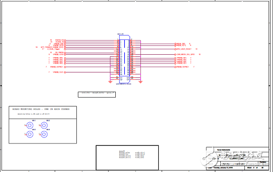
Figure 12. VisionSuper28 video application board circuit diagram (1)
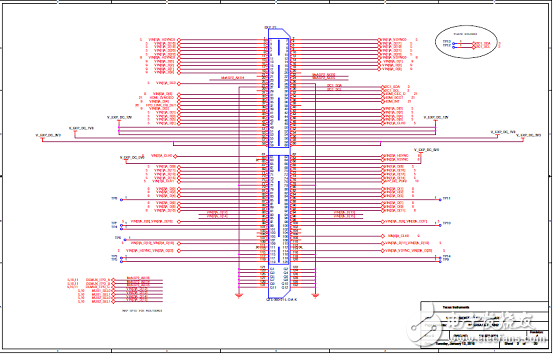
Figure 13. Circuit diagram of the VisionSuper28 video application board (2)
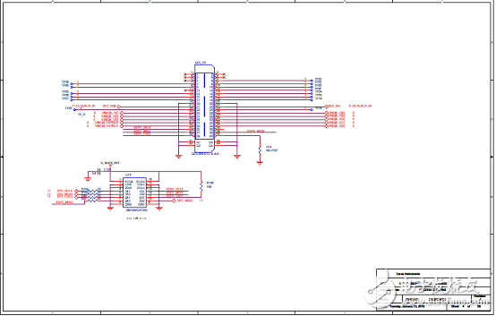
Figure 14. VisionSuper28 video application board circuit diagram (3)
Absolute rotary encoder measure actual position by generating unique digital codes or bits (instead of pulses) that represent the encoder`s actual position. Single turn absolute encoders output codes that are repeated every full revolution and do not output data to indicate how many revolutions have been made. Multi-turn absolute encoders output a unique code for each shaft position through every rotation, up to 4096 revolutions. Unlike incremental encoders, absolute encoders will retain correct position even if power fails without homing at startup.
Absolute Encoder,Through Hollow Encoder,Absolute Encoder 13 Bit,14 Bit Optical Rotary Encoder
Jilin Lander Intelligent Technology Co., Ltd , https://www.jllandertech.com