As long as the geometric shape of the nanostructure meets specific conditions and matches the wavelength of the incident light, the sensitivity of the optical sensor can be greatly improved. This is because local nanostructures can greatly amplify or reduce the electromagnetic field of light. According to a report by Memes Consulting, the youth research group "Nano-SIPPE" of HZB (Federation of German Helmholtz National Research Centers) led by Professor Christiane Becker is working on the development of such nanostructures. Computer simulation is an important tool for this type of research. Dr. Carlo Barth from the Nano-SIPPE team has now used machine learning to determine the most important field distribution patterns in nanostructures, and therefore explained the experimental results well for the first time.
Quantum dots on nanostructuresThe photonic nanostructure studied by the team consists of a silicon layer with a regular hole-like pattern, which is covered with a quantum dot coating made of sulfide. After laser excitation, the quantum dots close to the local field amplification emit more light than on the disordered surface. This can empirically prove how the laser interacts with the nanostructure.
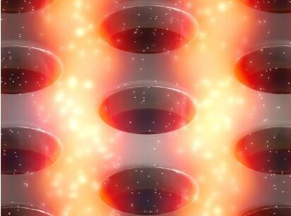
The computer simulation shows how the electromagnetic field is distributed in the silicon layer with hole-like patterns after laser excitation. As shown in the figure above, fringes with local field maximums are formed, so the quantum dots can emit light particularly intensely.
Ten different patterns discovered using machine learningIn order to systematically record what happens when the various parameters of the nanostructure change, Barth used software developed at the Zuse Institute in Berlin to calculate the three-dimensional electric field distribution of each parameter set. Then, Barth analyzed these massive amounts of data through other computer programs based on machine learning.
"The computer searched about 45,000 data records and divided them into about ten different patterns," he explained. Finally, Barth and Becker successfully identified three of the basic modes. In these three basic modes, the photoelectric magnetic field is amplified in each specific area of ​​the nanopore.
Outlook: Detect single molecules, such as cancer markersThis allows photonic crystal films based on excitation amplification to be optimized for almost any application. This is because according to different applications, for example, some biomolecules will preferentially accumulate along the edges of the nanopores, while other biomolecules will accumulate in the plateau area between the nanopores.
With proper geometry and accurate light excitation, the maximum electric field amplification can be accurately generated at the attachment position of the desired molecule. Its application is broad, for example, it can increase the sensitivity of the cancer marker optical sensor to a single molecule level.
Bluetooth Speakers,Bluetooth Speaker,Portable Speakers,Mini Speaker
Dongguan Guancheng Precision Plastic Manufacturing Co., Ltd. , https://www.dpowergo.com