As the number of components integrated in radio frequency integrated circuits (RFICs) continues to increase, so does the number of noise coupling sources, making power management increasingly important. This article describes the effects that power supply noise can have on RFIC performance. Although the examples in this article are the ADRF6820 quadrature demodulator with integrated phase-locked loop (PLL) and voltage controlled oscillator (VCO), the results are also applicable to other high-performance RFICs.
Power supply noise can create a mixture of frequencies in the demodulator, which can cause linearity degradation and adversely affect phase noise performance in the PLL/VCO. This article will detail the power evaluation scheme and provide a recommended power supply design using a low dropout regulator (LDO) and switching regulator.
With dual power supplies and ultra-high RF integration, the ADRF6820 is an ideal device for discussion. It uses an active mixing core similar to the ADL5380 quadrature demodulator, and the PLL/VCO core is identical to the ADRF6720, so the information provided in this article can also be used for these devices. In addition, the power supply design can also be used in new designs that require a 3.3 V or 5.0 V supply with similar power consumption.
The ADRF6820 quadrature demodulator and frequency synthesizer (shown in Figure 1) are ideal for next-generation communication systems. The device is feature rich, including a high linearity wideband I/Q demodulator, an integrated fractional-N PLL, and a low phase noise multi-core VCO. It also integrates a 2:1 RF switch, a tunable RF balun, a programmable RF attenuator and two LDOs. This highly integrated RFIC is available in a 6 mm &TImes; 6 mm LFCSP package.
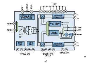
Figure 1. SIMRF6820 simplified functional block diagram
Power supply sensitivity
The modules most affected by power supply noise are the mixer core and the frequency synthesizer. Noise coupled into the mixer core can create unwanted signals, which can result in reduced linearity and dynamic range. This is especially important for quadrature demodulator because the low frequency mixing product is within the target band. Similarly, power supply noise can cause PLL/VCO phase noise performance to degrade. Unwanted mixing products and phase noise performance degradation are common problems with most mixers and frequency synthesizers, but the exact magnitude of the degradation depends on the architecture and layout of the chip. Understanding these power supply sensitivities helps to design a more robust power supply that optimizes performance and efficiency.
Quadrature demodulator sensitivity
The ADRF6820 uses a dual-balanced Gilbert cell active mixer core, as shown in Figure 2. Double balance means that both the LO and RF ports are differentially driven.
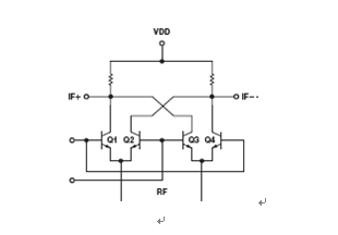
Figure 2. Gilbert cell double balanced active mixer
After the filter rejects higher order harmonics, the resulting mixer output is the sum and difference of the RF and LO inputs. The difference (also known as the IF frequency) is within the target band and is the desired signal. The sum terms are outside the band and are filtered.
Ideally, only the required RF and LO signals will be input to the mixer core, but this is rarely the case. Power supply noise can be coupled into the mixer input and behave as mixed spurs. The relative amplitudes of the mixing spurs may vary depending on the noise coupling source. Figure 3 shows an example mixer output spectrum. Due to the coupling of power supply noise, the mixing products with the wanted signal also appear on the output spectrum. In the figure, CW corresponds to a continuous wave or sinusoidal signal coupled to a power supply line. For example, the noise may be clock noise from a 600 kHz or 1.2 MHz switching regulator. Power supply noise can cause two different problems; if noise is coupled to the mixer output, the CW tone will appear at the output without any frequency conversion; if coupling occurs at the mixer input, the CW tone will modulate the RF and The LO signal and the product are generated at IF ± CW.
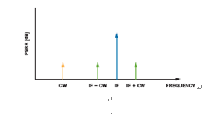
Figure 3. Example mixer output spectrum with power supply noise coupling
These mixing products may be close to the target IF signal, so it is difficult to filter them out, and dynamic range loss is unavoidable. This is especially true for quadrature demodulators because their baseband is complex and dc-centric. The demodulation bandwidth of the ADRF6820 ranges from DC to 600 MHz. If the mixer core is driven by a switching regulator with a noise frequency of 1.2 MHz, the unwanted mixing product will appear at IF ± 1.2 MHz.
Frequency synthesizer sensitivity
The references at the end of this article provide valuable information on how power supply noise affects integrated PLLs and VCOs. The principle applies to other designs that use the same architecture, but different designs require separate power evaluations. For example, an integrated LDO on the ADRF6820 VCO supply has greater noise immunity than a PLL supply that does not use an integrated LDO.
ADRF6820 power domain and power consumption
To design a power management solution, first consider the power domain of the RFIC to determine which RF modules are driven by which domain, the power consumption of each domain, the mode of operation that affects power consumption, and the power supply rejection of each domain. Using this information, the sensitivity data of the RFIC can be collected.
Each of the main functional blocks of the ADRF6820 has its own power supply pin. Both domains are powered by a 5 V supply. The VPMX drives the mixer core, and the VPRF drives the RF front end and input switches. The other domains are powered by a 3.3 V supply. VPOS_DIG drives an integrated LDO that outputs 2.5 V to drive the SPI interface, the PLL's Σ-Δ modulator, and the frequency synthesizer's FRAC/INT divider. The VPOS_PLL drives the PLL circuit, including the reference input frequency (REFIN), the phase frequency detector (PFD), and the charge pump (CP). VPOS_LO1 and VPOS_LO2 drive the LO path, including the baseband amplifier and the dc bias reference. VPOS_VCO drives another integrated LDO that outputs 2.8 V to drive a multicore VCO. This LDO is important for reducing sensitivity to power supply noise.
The ADRF6820 can be configured in a variety of operating modes. In normal operating mode, the power consumption is less than 1.5 mW with a 2850 MHz LO. Reducing the bias current reduces both power consumption and performance. Increasing the mixer bias current increases the linearity of the mixer core and improves IIP3, but reduces noise figure and increases power consumption. If the noise figure is important, the mixer bias current can be reduced, resulting in less noise and lower power consumption in the mixer core. Similarly, the baseband amplifier at the output has variable current drive capability for low impedance output loads. Low output impedance loads require higher current drive and higher power consumption. The data sheet lists some data sheets showing the power consumption in various operating modes.
Measurement steps and results
Noise coupling on the supply rail produces unwanted noise at CW and IF ± CW. To simulate this noise coupling situation, a CW tone is applied to each power pin to measure the amplitude of the resulting mixture of products relative to the input CW tone. The measured value is recorded as the power supply rejection capability in dB. Power supply rejection varies by frequency, so CW frequencies from 30 kHz to 1 GHz are scanned to capture specific behavioral data. The power supply rejection capability within the target band determines if filtering is required. The PSRR calculation method is as follows:
CW PSRR (unit: dB) = input CW amplitude (dBm) – CW feedthrough (dBm) measured at the I/Q output
(IF ± CW) PSRR (unit: dB) = input CW amplitude (dBm) – IF ± CW feedthrough (dBm) measured at the I/Q output
(IF + CW) (unit: dBm) = (IF – CW) dBm because the CW tones modulated around the carrier have equal amplitudes.
Lab setting
Figure 4 shows the lab setup. Apply a 3.3 V or 5 V DC source to the network analyzer to generate a swept continuous sinusoidal signal with an offset of 3.3 V or 5 V. This signal is applied to the various power rails on the RFIC. Two signal generators provide RF and LO input signals. Measure the output of the spectrum analyzer.
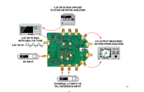
Figure 4. ADRF6820 PSRR Measurement Setup
Measuring step
The magnitude of the unwanted mix product depends on the power supply rejection of the chip and the size and location of the decoupling capacitors on the evaluation board. Figure 5 shows the amplitude of the output (IF + CW) tone, where a sinusoidal signal of 0 dB is given on the power supply pin. When there is no decoupling capacitor, the amplitude of the unwanted tone is between –70 dBc and –80 dBc. The data sheet recommends placing a 100 pF capacitor next to the front panel of the board and a 0.1 μF capacitor on the back. The resonance of these external decoupling capacitors can be seen from the figure. The transient at 16 MHz is the result of a 0.1 μF capacitor resonance (parasitic inductance is 1 nH). The transient at 356 MHz is the result of a 100 pF capacitor resonance (both capacitors have a parasitic inductance of 2 nH). The transient at 500 MHz is the result of a 100 pF capacitor resonance (parasitic inductance is 1 nH).
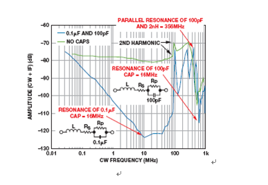
Figure 5. Effect of IF ± CW Decoupling Capacitor Resonance
result
The amplitude of the interfering signal (CW) and the modulated signal (IF ± CW) on the supply rail at the baseband output is measured. Noise is introduced on the power rail being tested, and other power supplies are kept clean. Figure 6 shows the amplitude of the (IF ± CW) tone when a 0 dB sinusoidal signal is injected into the power supply pin and swept in the 30 kHz to 1 GHz range. Figure 7 shows the feedthrough from the CW tone to the baseband output.
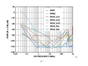
Figure 6. PSRR of (IF ± CW) tone 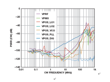
Figure 7. PSR for CW sound
analysis
The figure provides power sensitivity data at each power pin, which is very useful. VPOS_PLL has the worst power supply rejection and is therefore the most sensitive power supply node. The power pin drives the PLL circuit, including the reference input frequency, the phase frequency detector, and the charge pump. These sensitive functional blocks determine the accuracy and phase performance of the LO signal, so any noise coupled to it will propagate directly to the output.
Similarly, the VCO power supply can be considered as a very important node. As can be seen from the figure, the suppression performance of VPOS_VCO is far superior to VPOS_PLL. This is the result of the built-in LDO that actually drives the VCO. The LDO isolates the VCO from noise on external pins while providing a fixed noise spectral density. The PLL supply has no LDO and is therefore the most sensitive supply rail. It can be seen that isolating it from potential noise coupling is critical to achieving optimal performance.
The PLL loop filter attenuates the high CW frequency, so the VPOS_PLL is less sensitive at low frequencies and slowly improves when the frequency is swept from 30 kHz to 1 GHz. At higher frequencies, the amplitude of the interfering tone is attenuated and the power level injected into the PLL is significantly reduced. It can be seen that the high frequency power supply rejection performance of VPOS_PLL is superior to other power domains. The loop filter component is configured for 20 kHz as shown in Figure 8.
The supply rails (from highest sensitivity to lowest) are: VPOS_PLL, VPOS_LO2, VPOS_VCO, VPOS_LO1, VPOS_DIG, VPMX, and VPRF.
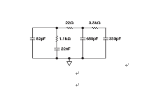
Figure 8. PLL loop filter configured for 20 kHz loop bandwidth
Power supply design
After the previous discussion, we have a good understanding of the maximum power consumption of the ADRF6820 in various modes and the sensitivity of each power domain. We use the switching regulator and LDO to design the power management solution to determine the two power solutions. The feasibility of the program. First, adjust a 6 V source to 5 V and 3.3 V for the ADRF6820 rail. Figure 9 shows the 5 V power supply design for VPMX and VPRF. The ADP7104 CMOS LDO can deliver up to 500 mA of load current. The ADP2370 low quiescent current step-down switching regulator operates from 1.2 MHz or 600 kHz. Additional filtering is added at the output of the switching regulator to attenuate switching noise. The ADP2370 can deliver up to 800 mA of load current. The 5 V rail of the ADRF6820 can be driven by the ADP7104 or ADP2370. Additional decoupling and filtering is applied to each power pin.
Figure 10 shows the 3.3 V power supply design. The source voltage is still 6.0 V, but an additional LDO drops the source voltage to the intermediate voltage and then the source voltage drops further to 3.3 V. An extra stage is required to reduce power loss because a maximum efficiency of 55% when operating from a 6 V source voltage directly down to 3.3 V. The switching regulator path does not require an intermediate stage because its pulse width modulation (PWM) architecture reduces power loss.
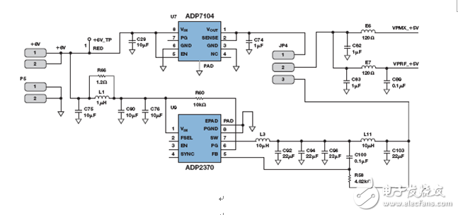
Figure 9. 5 V power supply design 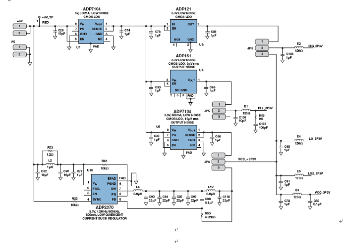
Figure 10. 3.3 V power supply design
The 3.3 V design allows for more experiments. In addition to driving a 3.3 V rail with an LDO or switching regulator, the VPOS_PLL rail has an additional LDO option and the VPOS_DIG rail has an optional isolated LDO. Due to the highest sensitivity of the PLL supply, we have tried three power solutions, each with different output noise: ADP151 3.3 V ultra-low noise CMOS LDO with 9 μV output noise; ADP7104 3.3 V low noise CMOS LDO, The output noise is 15 μV rms; the ADP2370 3.3 V buck regulator. We want to determine the highest power supply noise that still maintains the desired phase noise performance. Is the highest performance, lowest noise LDO indispensable?
An attempt was also made to use the ADP121 3.3 V low noise CMOS LDO on the VPOS_DIG rail to determine if digital noise would affect performance. Affected by the SPI interface switch, the noise of the digital power rail is generally higher than that of the analog power supply. We want to determine if the 3.3 V digital power supply requires its own LDO or can be directly coupled to an analog power supply. We chose the ADP121 as a low-cost solution.
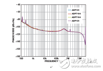
Figure 11. Integrated phase noise with ADP151 and ADP7104 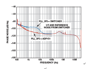
Figure 12. Integrated phase noise with ADP151 and ADP2370
Conclusion and recommended power supply design
For VPOS_PLL (the most sensitive supply rail), the low-cost ADP151 LDO achieves the same phase noise as the ADP7104 high-performance, low-noise LDO, as shown in Figure 11. However, when using the ADP2370 switching regulator, performance is degraded, as shown in Figure 12. The noise peak is caused by the switching regulator and is visible at its output, as shown in Figure 13. Therefore, the VPOS_PLL can withstand up to 15 μV rms of noise without causing a drop in integrated phase noise performance, but a switching regulator cannot be used to drive this pin. Using LDOs with higher performance and lower noise does not bring benefits.
Good phase noise performance is maintained when the remaining rails are driven with a switching regulator or LDO, as shown in Figure 14. The 5 V rail pins VMPX and VPRF can be connected and powered from a single supply. The 3.3 V supply pins VPOS_LO1, VPOS_LO2, and VPOS_VCO can also be connected and powered from a single supply. VPOS_DIG does not require a separate LDO and can be connected to an analog 3.3 V supply.
Figure 13. Output spectrum of the ADP2370 
Figure 14. Switch and LDO noise figure
The recommended power supply design (shown in Figure 15) uses a 6 V source voltage, including the ADP7104 5.0 V and the ADP7104 3.3 V LDO. This solution uses only LDOs because the source voltage is close to the required supply voltage. Efficacy is at an acceptable level, so there is no need to add additional filter components and switching regulators.
The recommended power supply design (shown in Figure 16) uses a 12 V source voltage, including two switching regulators and an LDO. The source voltage is much larger than the required supply voltage, so a switching regulator is used to improve efficiency. All power pins except the sensitive VPOS_PLL supply can be powered by a switching regulator. Both the ADP7104 or ADP151 can be used with VPOS_PLL.
references
Circuit Note CN0147 uses a low-noise LDO regulator to power a fractional-N voltage-controlled oscillator (VCO) to reduce phase noise, Analog Devices, Inc., 2010.
Collins, Ian, Integrated PLL and VCO [Part 2], Radio-Electronics.com, November 2010.
Modulator/demodulator
Linear regulator
Switching regulator
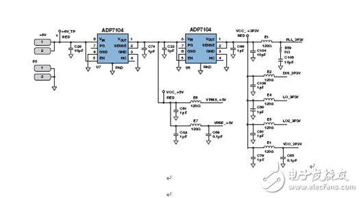
Figure 15. Recommended Power Supply Design for 6 V Source Voltage 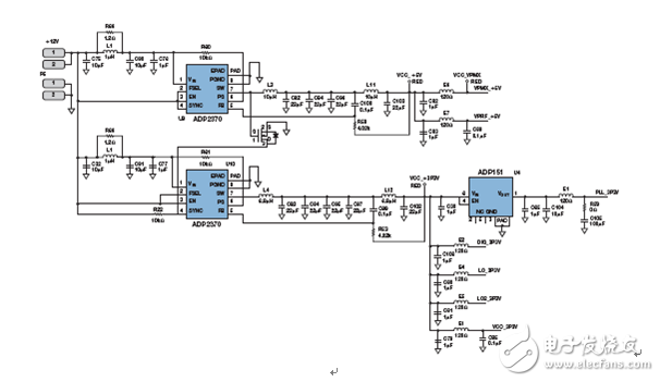
Figure 16. Recommended Power Supply Design for 12 V Source Voltage
Author: Qui Luu
Irradiated crosslinked polyethylene (PE-XC) pipe is a crosslinked pipe formed by extruding uncrosslinked polyethylene pipe and irradiated by electron accelerator or cobalt-60 radioactive source.
The crosslinking pipe produced by physical crosslinking method of electron accelerator has the obvious characteristics of uniform crosslinking degree, high purity, good health performance and reliable quality.
Crosslinked Pe Pipe,Pex Cross Linked Polyethylene,Cross Linked Polyethylene Tubing,Cross Linked Polyethylene Water Pipe
CAS Applied Chemistry Materials Co.,Ltd. , https://www.casac1997.com