Organic thin films and metal thin films of OLED devices and water and air will immediately oxidize and deteriorate, so measures must be taken to avoid this problem. The inorganic film protection method may be used. The inorganic film protection material includes silicon nitride, magnesium fluoride, indium oxide, etc., and the inorganic protective film material is prepared by a resistance heating method or a magnetron sputtering method. After the protective film is formed, the fabricated device is packaged, and the encapsulation process must be carried out in an anhydrous, oxygen-free inert gas, and the encapsulating material includes a binder and a covering material. The adhesive uses an ultraviolet curing or heat curing epoxy curing agent, the covering material is covered with a glass, and a desiccant is added to the cover to adsorb residual moisture.
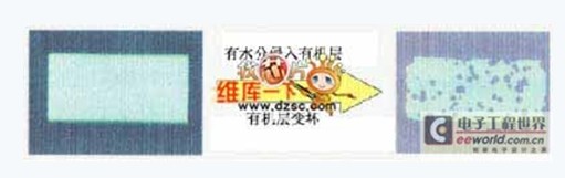
The picture below shows: damage caused by moisture intrusion into the organic layer
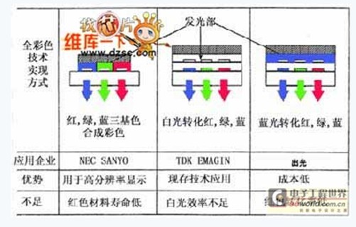
3. White light device + color filter mode
The earliest technology to carry out this technology was TDK Corporation of Japan, where the light emitted by the white light device was colored by a color filter. The color filter has higher cost and low luminous efficiency. Although this mode can obtain high color purity, the aging characteristics of the red, green and blue trichromatic optical devices are different, and the color purity changes with time.
The following picture shows three colorization schemes:
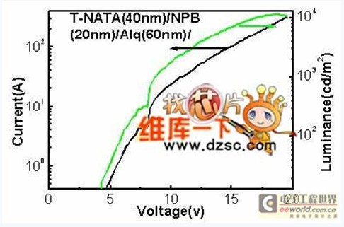
Packaged OLED devices must be characterized for characterization, primarily luminance-voltage curves and current density-voltage curves. The steeper the curve rises, the faster the luminous brightness increases with voltage and current density with voltage, and the higher the luminous efficiency.
Current density-voltage curve
Edit: Nizi
Usb Common Mode Choke,Magnetic Ring Inductor,Wurth Inductor,Coilcraft Inductor
IHUA INDUSTRIES CO.,LTD. , https://www.ihua-inductor.com