Introduction The MAX3420E can be connected to any SPI host controller to form a full-speed USB peripheral device. Although the MAX3420 manages the underlying USB signaling, the SPI host controller must be involved in the processing of USB events. The INT pin of the MAX3420 indicates that an interrupt has occurred, and the SPI main controller reads 14 interrupt request bits to determine the interrupt that needs to be serviced. These interrupt request (IRQ) bits determine the working process of the MAX3420E. Note: The SPI host controller can be a microcontroller, DSP, ASIC, or any device with an SPI port, and can provide the SCLK signal. The terms "SPI master controller" and "microcontroller" used in this document have the same meaning. MAX3420E interrupt logic
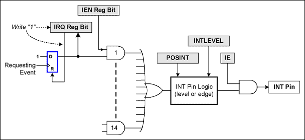
Figure 1. The MAX3420E interrupt logic. The shaded parts are the register bits.
Figure 1 shows the MAX3420E interrupt logic. The shaded parts are the register bits accessible via SPI.
Each interrupt source in the IRQ bit has a trigger for latching service requests. The output of the flip-flop is IRQ, which appears in the MAX3420E register. The IRQ bit provides two functions:
Reading an IRQ bit will return the status of the IRQ trigger. Writing a "1" to the IRQ bit will clear the IRQ trigger, and writing a "0" to the IRQ bit will not change the trigger state. The IRQ bit can be read at any time, it reflects the state of the IRQ trigger. According to item 2 above, write 1 instead of 0 to clear the selected IRQ bit. This process does not require a read-modify-write cycle. For example, suppose that the IRQ bit of the MAX3420E is the same as the ordinary register bit, write 1 to set, write 0 to clear. Now, we want to clear the UERSIRQ bit of the USBIRQ register. Figure 2 shows the code for this operation.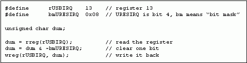
Figure 2. Clearing general register bits requires one RMW operation
Because the SPI host controller clears a MAX3420E IRQ bit by writing 1, and writing 0 does not change other register bits, the SPI host controller can directly write the bit mask value to clear the UERSIRQ bit. Therefore, the last three sentences in Figure 2 can be replaced by the single sentence in Figure 3.

Figure 3. A register write operation to clear the MAX3420E IRQ bit
IEN bit
Each of the 14 MAX3420E interrupts has a corresponding interrupt enable (IEN) bit. The IEN bit and the IRQ trigger output are ANDed to determine whether to send an interrupt request to the INT pin (Figure 1). After the 14 IRQ triggers pass the gate control circuit, they perform an "OR" operation to form an internal interrupt request signal, which is transmitted to the interrupt pin logic module.
Note that regardless of the state of the IEN bit, the IRQ bit indicates the interrupt suspension state. In this way, even if the interrupt does not trigger the INT pin, the firmware can still check the suspended interrupt. If your program needs to check whether an IRQ register "suspends interrupts", a simple method is to read the IRQ and IEN registers, perform an AND operation on them, and check the bits that now indicate "waiting and enabled IRQ". A value of zero indicates that an interrupt that is not enabled is in a suspended state.
IE bit
The SPI master controller enables or disables the INT pin through the IE bit. Since this bit affects all interrupts, it is usually called global interrupt enable. Regardless of the state of the IRQ or IEN bit, when IE = 0, the INT pin is invalid.
The interrupt pin logic two register bits INTLEVEL (refer to the discussion below) and POSINT control the working mode of the INT pin. Before setting IE = 1, these two configuration bits should be set first.
Level mode, INTLEVEL = 1
Some microcontroller systems use active low interrupts. In this configuration, the MAX3420E uses an open-drain transistor to drive the INT pin to ground. Since the pin can only be driven low, a pull-up resistor needs to be connected between the INT pin and the logic power supply. This mode supports the INT pin output of multiple chips (each is an open-drain output) connected together, and uses a single pull-up resistor. Since any chip output can pull this pin low, this logic is sometimes called a "wire OR". For this type of system, set INTLEVEL = 1.
Edge mode, INTLEVEL = 0 (default)
The MAX3420E INT pin can also drive an edge-active interrupt system, at which time the microcontroller checks the 0-1 or 1-0 transition on its interrupt input pin. This is the default mode of the MAX3420E, INTLEVEL = 0. The SPI master controller sets the edge polarity through the second POSINT bit. When POSINT = 1, the MAX3420E outputs a 0-1 transition for the suspension interrupt. When POSINT = 0 (default), the MAX3420E outputs a 1-0 transition for the suspension interrupt.
In Figure 1, please note the following:
If an IRQ bit is set and the corresponding IEN bit is cleared, IRQ will not affect the INT output pin. However, the interruption is still suspended. You can always read the IRQ bit to obtain its status. You can write 1 to the corresponding register bit to clear the IRQ bit. The IEN bit of the suspended interrupt (IRQ bit is 1) will generate an interrupt when the 0-1 transition occurs. The INT pin can be connected to the interrupt system of the microcontroller. In addition, the microcontroller can poll the INT pin to determine whether the MAX3420E has an interrupt in the suspended state. The most suitable mode for polling is level mode (INTLEVEL = 1), because in edge mode, the pulse output from the INT pin may be too narrow for the microcontroller to detect (refer to the discussion below). Please note that the level mode requires a pull-up resistor between the INT pin and VL. INT pin waveform level mode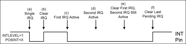
Figure 4. MAX3420E INT pin change in level mode (INTLEVEL = 1)
Figure 4 shows the MAX3420E INT pin waveform in level mode. The INT pin is statically high (pulled up to VL). Assuming the IEN position of the two interrupts in the figure is 1, and the global IE position is 1, then the following events will occur. (The items marked with letters below correspond to the events marked with the same letters in Figure 4.)
An interrupt request occurs, bringing the MAX3420E INT pin low. Note: Although the MAX3420E interrupt output pin is called the INT pin, it is sometimes negative (for example, in level mode). After the SPI master controller completes the interrupt service, write 1 to the IRQ bit to clear it. The INT pin returns to a static high level. The interval between (a) and (b) is the time between the interrupt setting its IRQ bit and the SPI master clearing the IRQ bit. Another interrupt request is generated and the INT pin is pulled low. When the first interrupt request is in a suspended state, a second interrupt request is generated. There is no change in the INT level because at least one interruption is suspended. (Actually, there are two interrupts in the suspended state at this moment.) After the SPI main controller completes an interrupt service, write 1 to the IRQ bit to clear it. Since there is still an interrupt in the suspended state, the INT pin remains low. The SPI master controller processes the remaining interrupt requests, writes 1 to the IRQ bit, and clears it. No interrupt is in a suspended state, so the INT pin returns to a static high level. Note: If an interrupted IRQ trigger (Figure 1) is set, the interrupt is considered to be in a suspended state.This logic can handle INT pin polling well. If any part of the MAX3420E needs to be serviced, and its interrupt has been enabled, then the INT pin goes low. The INT pin remains low until the microcontroller clears the last suspended IRQ bit.
Edge mode
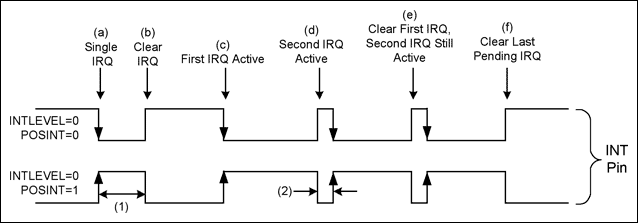
Figure 5. The MAX3420E INT pin changes in edge mode (INTLEVEL = 0). The interval (1) is the time for the SPI master to clear the IRQ, and the interval (2) is 10.67 µs.
Figure 5 shows the waveform of the MAX3420E INT pin in two polar edge modes. The polarity is controlled by the POSINT bit. The waveform is similar to the level mode, but there are two differences. Under two conditions, the INT pin generates an edge transition:
An IRQ bit becomes active (its IRQ flip-flop produces a 0-1 transition). The processor clears an IRQ bit (writes 1 to it), and the other IRQs are in a suspended state. The second condition ensures that the processor can detect edge transitions when there are interrupts to be serviced.In addition to generating edge transitions, as in level mode, the INT pin also has active and inactive states. The invalid state of the INT pin depends on the edge polarity set by the POSINT bit. At this point, the edge mode is similar to the level mode. You can know whether there is an interrupt in the suspended state by checking the state of the INT pin:
In negative edge mode, if there is no suspension interrupt, the INT pin is high; if there is suspension interrupt, it is low. In positive edge mode, if there is no suspension interrupt, the INT pin is low; if there is suspension interrupt, it is high. The following explanation explains the valid and invalid states of the INT pin. The valid state means that at least one interruption is in the suspended state; the invalid state means that no interruption is in the suspended state. Assuming that the interrupt has been enabled, the following events will occur. (The items marked with letters below correspond to the events marked with the same letters in Figure 5.) When an interrupt request is generated, an edge transition occurs on the MAX3420E INT pin. The polarity of the edge depends on the setting of the POSINT bit. Because the interrupt is still suspended, the INT pin remains in its active state. After the SPI master controller completes the interrupt service, write 1 to the IRQ bit to clear it. The MAX3420E INT pin returns to the inactive state. The interval (1) between (a) and (b) in the figure is the time between the generation of an interrupt and the IRQ bit cleared by the SPI master. When another interrupt request is generated, the MAX3420E INT pin generates an edge transition and maintains its active state. When the first interrupt request is in a suspended state, a second interrupt request is generated. The MAX3420E INT pin must generate another edge transition, so this pin generates a transition pulse between the inactive and active states to provide the correct edge polarity. In the MAX3420E, the pulse width is fixed at 10.67µs. Because there are still interrupts in the suspended state, the INT pin remains in the active state. After the SPI master controller completes a suspension interrupt service, write 1 to its IRQ bit to clear it. As in step (d), the INT pin generates another edge transition. The SPI master controller processes the remaining interrupt requests, writes 1 to its IRQ bit, and clears it. No interrupt is in the suspended state, therefore, the INT pin returns to the inactive state. Interrupt Register Table 1. The shaded MAX3420E register bits control the interrupt system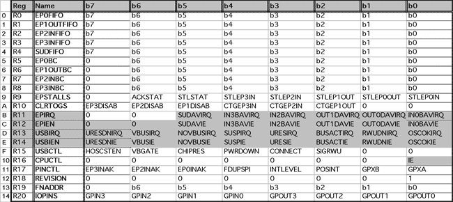
The MAX3420E has two types of USB interrupts, which are controlled by the shaded registers in Table 1. There are two types of interrupt bits: endpoint control located in the EPIRQ (R11) and EPIEN (R12) registers, and USB control located in the USBIRQ (R13) and USBIEN (R14) registers. The global IE bit is in the CPUCTL register.
Table 2. 14 MAX3420E interrupt sources
| Bit Name | Default | LocaTIon | Set By | Cleared By |
| IN0BAVIRQ | 1 | EPIRQ.0 | EP0 FIFO is ready for µP loading | Load the EP0BC register |
| OUT0DAVIRQ | 0 | EPIRQ.1 | EP0-OUT FIFO has host data | Write EPIRQ = 0x02 |
| OUT1DAVIRQ | 0 | EPIRQ.2 | EP1-OUT FIFO has host data | Write EPIRQ = 0x04 |
| IN2BAVIRQ | 1 | EPIRQ.3 | EP2-IN FIFO is ready for µP loading | Load the EP2INBC register |
| IN3BAVIRQ | 1 | EPIRQ.4 | EP3-IN FIFO is ready for µP loading | Load the EP3INBC register |
| SUDAVIRQ | 0 | EPIRQ.5 | Setup Data is available in SUDFIFO | Write EPIRQ = 0x20 |
| OSCOKIRQ | 0 | USBIRQ.0 | MAX3420E Oscillator / PLL is stable | Write USBIRQ = 0x01 |
| RWUDNIRQ | 0 | USBIRQ.1 | SIE has finished signaling RWU | Write USBIRQ = 0x02 |
| BUSACTIRQ | 0 | USBIRQ.2 | Bus is acTIve | Write USBIRQ = 0x04 |
| URESIRQ | 0 | USBIRQ.3 | Host started signaling bus reset | Write USBIRQ = 0x08 |
| SUSPIRQ | 0 | USBIRQ.4 | Host suspended the bus | Write USBIRQ = 0x10 |
| NOVBUSIRQ | 0 | USBIRQ.5 | VBUS comparator made 1-0 transiTIon | Write USBIRQ = 0x20 |
| VBUSIRQ | 0 | USBIRQ.6 | VBUS comparator made 0-1 transition | Write USBIRQ = 0x40 |
| URESDNIRQ | 0 | USBIRQ.7 | Host finished signaling bus reset | Write USBIRQ = 0x80 |
Table 2 shows the 14 interrupt control bits, when the MAXQ3420E internal logic sets them, and how the SPI master controller clears them. Interrupt request bit BAV bit Three buffer ready (BAV) IRQ bit indicates that the SPI host controller can be loaded into an IN endpoint FIFO. After the chip is reset or the IN data is successfully sent from the endpoint buffer to the host, the MAX3420E sets these IRQ bits. This IRQ informs the SPI main controller that the buffer can be loaded with new data.
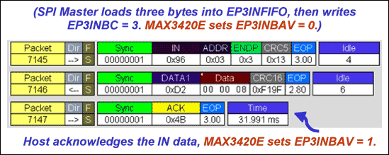
Figure 6. Host process of sending an IN request to endpoint 3
Figure 6 shows the bus process for IN transmission. The host applies for data from the MAX3420E. Before the data packet 7145 arrives, the SPI host controller first loads byte 00 00 08 into the endpoint 3-IN FIFO (EP3INFIFO). Then, the SPI host controller writes the value 3 to the EP3INBC (Endpoint 3 IN byte count) register. Write the byte count register to complete the following three functions:
Tell the MAX3420E how many bytes to send when an IN request arrives. Prepare the endpoint for data transmission (not non-response). Clear the EP3INBAV IRQ bit. The MAX3420E responds to the IN data packet with the endpoint 3 as the address with the data packet 7146. The host sends an acknowledgement (ACK) packet 7147 in response to the received error-free data. When the MAX3420E detects the host ACK packet, it sets the EP3INBAV interrupt request bit to inform the SPI host controller that the endpoint FIFO can load new data.If the IN packet arrives before the SPI master controller is ready for the endpoint, the MAX3420E will respond with a NAK handshake signal (Figure 7). The NAK handshake signal informs the host to resend the IN request later.
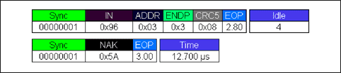
Figure 7. If the MAX3420E is not ready to send data, then send out a NAK packet.
If an error occurs during the transmission of IN data to the host, when the host retransmits the IN request, the MAX3420E automatically retransmits the data (and the same data triggers DATA0 / DATA1). Only after receiving the ACK handshake signal from the host, the MAX3420E will set the BAV IRQ bit of the endpoint, indicating that the buffer is ready to receive new data.
Important note: As with all MAX3420E IRQ bits, the BAV IRQ bit can also be cleared by writing 1 to three. Never do this. Instead, use the method listed above: clear the BAV IRQ bit by writing to the byte count register of the IN endpoint. This is because the MAX3420E uses the BAV interrupt request bit of an IN endpoint as the locking mechanism. This mechanism ensures that the SPI host controller and the MAX3420E serial interface engine (SIE) will not use the endpoint buffer at the same time. For example, if the BAV bit is cleared and then the byte counter is loaded with two separate instructions, then when you update the byte count register, the packet transmission may begin, resulting in data errors.The default value of BAV IRQ The default value of the three BAV IRQ bits (see 1 in the Default column of Table 2) is 1. This indicates that the SPI master controller will read EPIRQ = 0x19 after power-on or reset. If any corresponding IEN bit is set, the INT pin will indicate that the interrupt is in a suspended state.
Double buffered endpoint EP2-IN
The MAX3420E EP2-IN endpoint is a double-buffered structure. This shows that it has two sets of 64-byte FIFO and byte count registers. Double buffering increases the transmission bandwidth because the SPI host controller does not need to wait for the data packet to be transferred to the host before loading another data packet. With the double-buffer structure, the SPI master controller can load one IN FIFO into another IN FIFO while transmitting its IN data to the host. When you load the EP2INBC register, the two buffers "automatically rotate". This provides another FIFO (second group) and byte count register to the SPI master controller. This double buffering mechanism is transparent to the firmware.
The double buffering mechanism allows us to observe that the only effect occurs during the initialization process. At power-up or chip reset, the IN2BAVIRQ bit is set. Under normal circumstances, the initialization program loads the data into the EP2IN FIFO, and then loads the EP2INBC register to prepare for transmission and clears the IN2BAVIRQ bit. When you do this, you will find that the MAX3420E immediately resets the IN2BAVIRQ bit. This indicates that the second buffer is ready, allowing the SPI host controller to load the second packet.
DAV interrupt request bit
The data ready (DAV) IRQ bit of the OUT endpoint indicates that new data has been received from the host. The MAX3420E automatically handles the bus retry operation, and only when the received data has no error codes, an interrupt request will be generated. When the SPI host controller receives the DAV interrupt request, it will read the endpoint byte count register to determine the size of the valid data. Then the SPI master controller reads the corresponding number of bytes from the OUTFIFO of the endpoint. The SPI master clears the OUTDAV IRQ bit in the normal way by writing 1 to it. In this way, the endpoint is ready again to receive the next OUT packet.
In Figure 8, the host sends an OUT PID and four bytes of data, and the MAX3420E transfers it to the EP1OUT FIFO. When the MAX3420E verifies that the transmission is error-free, it will update its EP1OUTBC register to indicate four bytes, send an ACK packet to the host, and set EP1OUTDAV IRQ to notify the SPI host controller that it can extract the data that has been prepared in the endpoint 1 FIFO.
Figure 8. Bus process where the host sends an OUT packet to endpoint 1
Double buffered endpoint EP1-OUT
The MAX3420E EP1-OUT endpoint is a double-buffered structure, which indicates that it has two sets of 64-byte FIFO and byte count registers. Double buffering means that after the SPI master clears OUT1DAVIRQ, if there is another host data packet waiting, it can be reset immediately.
SUDAV interrupt request bit When the host sends a CONTROL transmission to the MAX3420E, the MAX3420E stores 8 SETUP bytes in an 8-byte FIFO, and the SPI master controller can read the data from the SUDFIFO register. Because peripherals always receive host data from this buffer, SUDAVIRQ acts like an OUT endpoint FIFO. When new data from the host is received, the MAX3420E sets its SUDAV IRQ. A SETUP packet always contains 8 bytes, so SETUP data does not require a byte count register.
OSCOK interrupt request bit When the MAX3420E is powered on, the chip is reset, or exits the power-off state, it takes time to start the internal oscillator and PLL to achieve stability. Oscillator ready (OSCOK) IRQ indicates that the MAX3420E is ready to work.
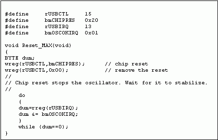
Figure 9. Sample code to reset the MAX3420E and wait for OSCOK before ending.
Figure 9 shows example code that uses the CHIPRES register bits to reset the MAX3420E. Since the chip reset will stop the internal oscillator, after setting the code CHIPRES = 0 to clear the reset signal, you should wait for the oscillator to stabilize before using the MAX3420E.
When the RWUDN interrupt request bit is in the suspended state, the USB peripheral can issue a remote wake-up (RWU) signal to notify the host to resume bus operation. The USB specification defines a remote wake-up signal of 1ms to 15ms K-state. The SPI master controller triggers the RWU signal by setting the remote wake-up signal (SIGRWU) bit equal to 1.
When the SPI master sets the SIGRWU bit, the MAX3420E waits 5ms, drives the K-state for 10ms, and then sets the remote wakeup complete interrupt request (RWUDNIRQ) bit. The 5ms delay is guaranteed to meet another USB requirement: the bus must be idle (J-state) for at least 5ms before the peripheral device sends a resume signal.
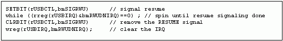
Figure 10. Example code to send remote wakeup signal
Figure 10 shows the example code for sending a remote wake-up. Note that the MAX3420E implements signal timing and sets IRQ after completion. The MAX3420E handles all timed USB events in such a way that an interrupt is generated when completed, so the SPI host controller does not require timing control signal intervals.
The code in Figure 10 sets the SIGRWU bit, and then waits for RWUDNIRQ to be set to determine the signal duration of 10ms. Then, the SPI master sets SIGRWU = 0 and clears the IRQ bit. In general, in a multitasking SPI master controller, it should respond to the RWUDNIRQ interrupt request without having to waste time directly checking the IRQ bit.
Within 5ms after receiving the RWUDNITQ interrupt, the SPI master should turn off the SIGRWU bit. If this is not done, the MAX3420E will start another 10ms K-state and repeat the process (wait 5ms, then 10ms K-state) until SIGRWU = 0. Setting SIGRWU = 0 during RWU signal processing will not terminate the RWU signal.
If the SPI main controller sets SIGRWU = 1 when the MAX3420E is in the power-off state (PWRDOWN = 1), then the MAX3420E will automatically restart the oscillator, wait for it to stabilize, and then start sending RWU signals. In this case, the SPI host controller does not need to check the OSCOK IRQ.
BUSACT interrupt request bit When the MAX23420E detects a SYNC mode at the beginning of the USB packet, it sets the BUSACT IRQ bit. The USB bus reset process is not a bus active state, so it will not trigger a BUSACK interrupt request.
URES and URESDN interrupt request bits
The USB host resets the peripherals by maintaining the single-ended zero (SE0) state for at least 50 ms (D + and D- are driven low simultaneously). After detecting a 2.5µs SE0 state, the MAX3420E sets the USB reset IRQ (URESIRQ). Then, when the host completes the reset, the MAX3420E sets the USB reset completion IRQ (URESDNIRQ).
Because the SPI host controller needs to monitor the USB bus reset event, the MAX3420E will not clear the URESIE, URESDNIE, or IE interrupt enable bit during the bus reset. But during bus reset it will clear all other interrupt enable bits in the EPIEN and USBIEN registers.
SUSP interrupt request bit When the MAX3420E detects that the bus has stopped working for 3ms (continuous J-state), it generates a suspend interrupt request (SUSPIRQ). If the peripheral device using the MAX3420E is powered by the bus, it must enter a low-power state to minimize the current drawn from VBUS. In this case, the SPI master controller should shut down the power-consuming peripherals, and then set PWRDOWN = 1, so that the MAX3420E enters low-power mode. As a result, the MAX3420E oscillator stops working and enters the lowest power state.
Need to pay attention to the following two programming tips:
Clearing the SUSPIRQ bit cannot prevent the interrupt from regenerating after 3ms. When the bus is suspended, to avoid repeated suspension interrupts, the suspended IEN bit should be cleared before the bus resumes operation. The internal suspend timer logic is clocked by the MAX3420E's internal oscillator. Therefore, if you put the device into shutdown mode (set PWRDOWN = 1) and then try to clear the bit by writing 1 to the SUSPIRQ bit, the MAX3420E will not clear the bit. The MAX3420E is inseparable from the internal clock that has now stopped working. VBUS and NOVBUS interrupt request bits A self-powered peripheral can detect whether it is plugged into the USB interface and use these interrupts to power on. The internal VBUS comparator triggers these interrupts. It compares the VBCOMP pin voltage with the internal reference voltage. They are all edge-triggered and are set when the VBUS voltage (VBUSIRQ) is powered or stopped (NOVBUSIRQ).The bus-powered peripheral does not need to detect VBUS because it is powered by VBUS. In this way, the VBCOMP pin can be released and used as a general purpose input. In this application, the VBCOMP pin has no internal pull-up resistor, so a pull-up resistor should be connected between the VBCOMP pin and VL.
Programming Tip Clear IEN Bit Chip Reset During chip reset, all IE bits are cleared. The chip resets when the following conditions occur: The VL power supply powers the MAX3420E (power-on reset). The MAX3420E RES # pin is set low. The SPI master controller sets CHIPRES = 1. Bus reset When the MAX3420E detects a USB bus reset (bus pause for 3ms), all three IE bits are cleared except the three IE bits. The SPI host controller may need to handle the bus reset interrupt to monitor the status of the bus reset signal. Therefore, the bus reset does not affect the following IE bits: URESIE URESDNIE IE (Global Interrupt Enable) Since the USB bus reset clears most of the IE bits, after the bus is reset, the control firmware should re-enable the required interrupt.Clear the BAV and DAV IRQ bits. Please note that the DAV IRQ bit is cleared in the normal way of writing 1. The BAV bit (used for the IN endpoint) is cleared differently, and the method used is to write to the byte count register.
Ultra Thin Battery,Ultra Slim Battery Pack,Thin Lithium Ion Battery,Ultra Light Optics Battery,Polymer lithium battery,Cylindrical Lithium Battery
Langrui Energy (Shenzhen) Co.,Ltd , https://www.langruienergy.com