Abstract: Crosstalk is an important concept in SI design. How to keep the signal from being affected by surrounding signals during the transmission process in product design, and not affecting other signal lines, is the key to ensuring that the product passes the test smoothly. The generation of crosstalk is mainly due to the mutual capacitance and mutual inductance between adjacent transmission lines. These distributed parameters enable the signal to partially couple the voltage and current information carried by itself to the adjacent disturbed during the transmission process. Line (Victim line). At present, the commonly used methods of suppressing crosstalk are based on the principle of reducing the distribution parameters between lines. For example, simply open the wire spacing (common 3W principle), add protective wires, protective ground holes, etc.; for the crosstalk that exists between the wiring harnesses, the crosstalk amplitude is usually reduced by twisting and shielding. This article will introduce the effects and differences of these common measures in detail, and hope that through analysis from different perspectives, readers can understand some of the methods in product design.
table of Contents
Crosstalk
1. Near-end crosstalk and far-end crosstalk
2. The establishment of crosstalk model
3. The influence of coupling length on crosstalk (multiple crosstalk)
4. The influence of pitch change on crosstalk (origin of 3W principle)
5. The influence of the protective ground wire on crosstalk (Guard Trace Effect)
6. The impact of protective vias on crosstalk
7. Minimization of Crosstalk
8. ANSYS crosstalk check module
9. Crosstalk between cables
reference
1. Near-end crosstalk and far-end crosstalk
Crosstalk is caused by the coupling of energy from one line to another, and the coupling methods are mainly divided into electric field (electric field) and magnetic field (magnetic field). Due to the mutual capacitance and mutual inductance between the traces, the AC signal on one trace will be transferred from these distributed mutual capacitance and mutual inductance to the victim net. .
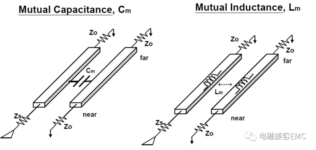
Fig1. Mutual Capacitance and Mutual Inductance
1.1 Mutual inductance
The mutual inductance guides the noise current from one drive line to the adjacent disturbed line through the magnetic field, and the magnetic field lines generated by the drive line pass through the disturbed line to form an induced current.
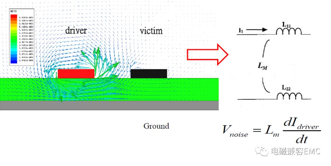
Fig2.Mutual Capacitance
1.2 Mutual capacity
It is the electric field coupling between the two conductors, and the time-varying voltage signal on the drive line induces an induced voltage on the disturbed line through mutual capacitance.
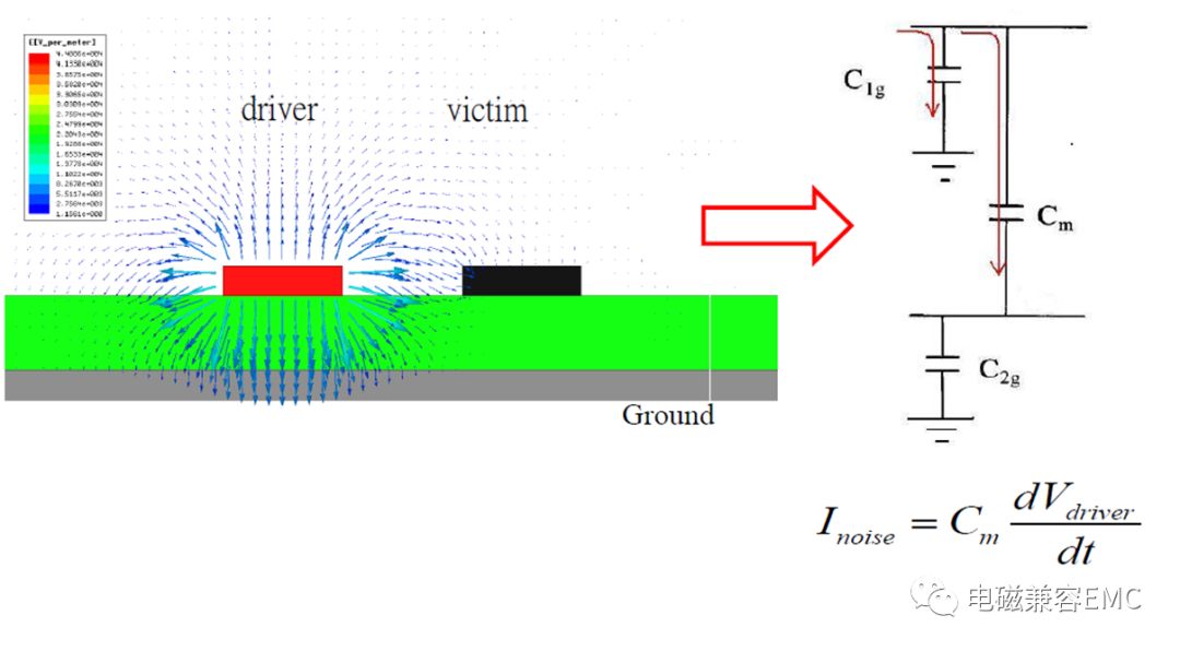
Fig3.Mutual Inductance
1.3 Near-end crosstalk and far-end crosstalk
As shown in Figure 1, in reality, in order to measure the amplitude of crosstalk, the noise at both ends of the victim line is measured separately. In order to distinguish the two ends, the end closest to the source is called the "near end", and the end far away from the source is called the "near end". The farthest end is called the "distal". The two ends can also be defined by the direction of signal transmission, that is, the far end is the "front" of the signal transmission direction, and the near end is the "rear" of the signal transmission direction. The noise coupled on the victim line is divided into current noise and voltage noise. The figure below is a schematic diagram of the noise current coupled on the victimline. The NEXT near-end coupling current is the sum of the mutual inductance coupling current and the mutual capacitance coupling current. On the contrary, the FEXT far-end coupling current is the difference between the mutual inductance coupling current and the mutual capacitance coupling current.
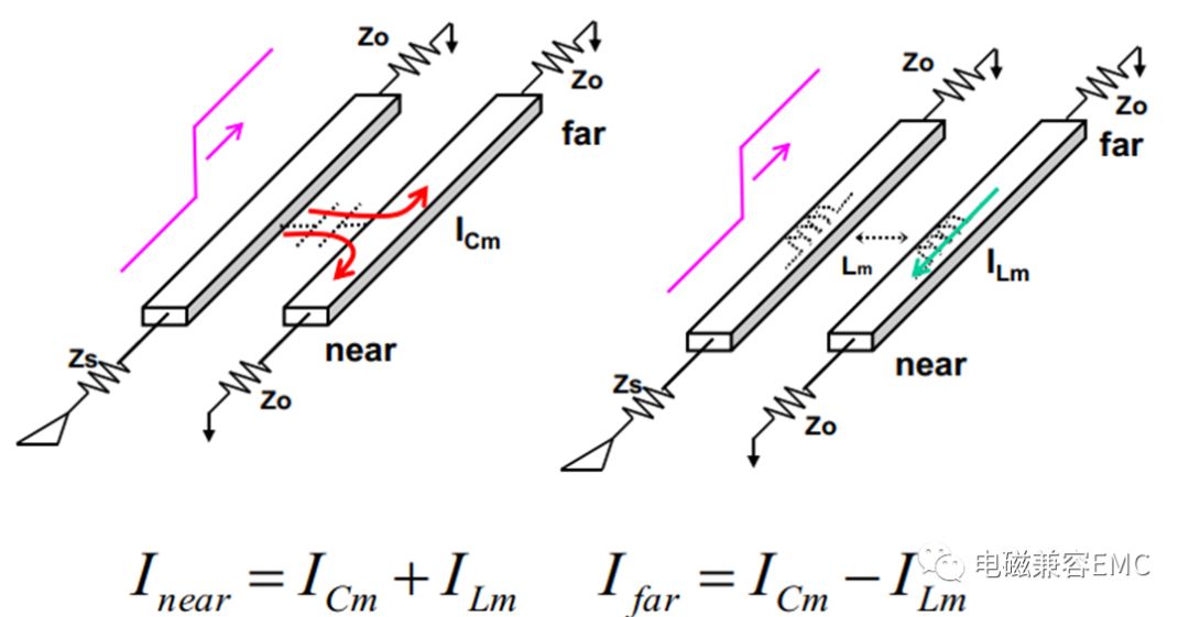
Fig4. Coupled Currents
The figure below is a schematic diagram of voltage coupling. From Figure 4, it can be seen that near-end crosstalk is the sum of mutual capacitance and mutual inductance current, so the voltage amplitude of near-end crosstalk is always positive. The far-end crosstalk is the difference between the mutual capacitance and the mutual inductance current, so the far-end crosstalk is not always negative. There are two reasons:
The current of Lm is greater than the current of Cm
When the remote end is open
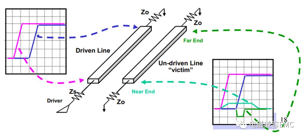
Fig5 Schematic diagram of voltage coupling
For the description of the near-end and far-end coupling voltages, the following picture of teacher Wu Ruibei's courseware gives the crosstalk models and corresponding calculation formulas for the near-end and far-end under three situations. It can be seen that the amplitude of the near-end coupling noise is only related to the microstrip line distribution parameters and the driving voltage. When the cross-sectional size of the coupled microstrip line and the driving voltage level are determined, its amplitude can be determined. The amplitude of the remote coupling noise is not only related to the microstrip line distribution parameters and the driving voltage, but also related to the time delay and the rising edge time of the driving waveform.
The driver pluse causes a long coupling signal at the near end of the quiteline. The signal starts at time 0 and lasts for 2Td. The near-end crosstalk signal gradually rises with the rising edge of the driver. When the leading edge of the signal is transmitted for a certain length, the near-end The current will reach a stable value and no longer increase. This length is called the saturation length. The saturated length of the transmission line Len is:
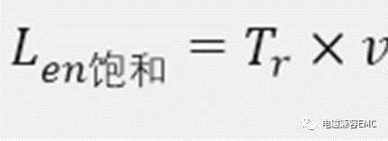
Among them is the signal rise time, and v is the transmission speed of the signal in the driver line.
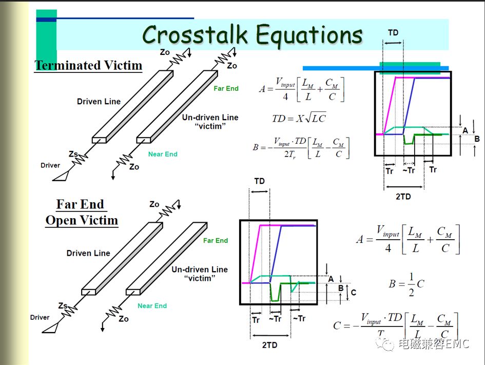

Fig6 NEXT and FEXT waveform and amplitude calculation
2. The establishment of crosstalk model
Because there is no ideal transmission line in reality, impedance matching under ideal conditions cannot be achieved, so it can be said that reflection is everywhere. The existence of reflection complicates the analysis of crosstalk. Therefore, in order to reduce its influence, it is necessary to design the impedance of the established model to minimize the amplitude of the reflection.
2.1 Use ANSYS Microstrip-CPL tool for characteristic impedance design
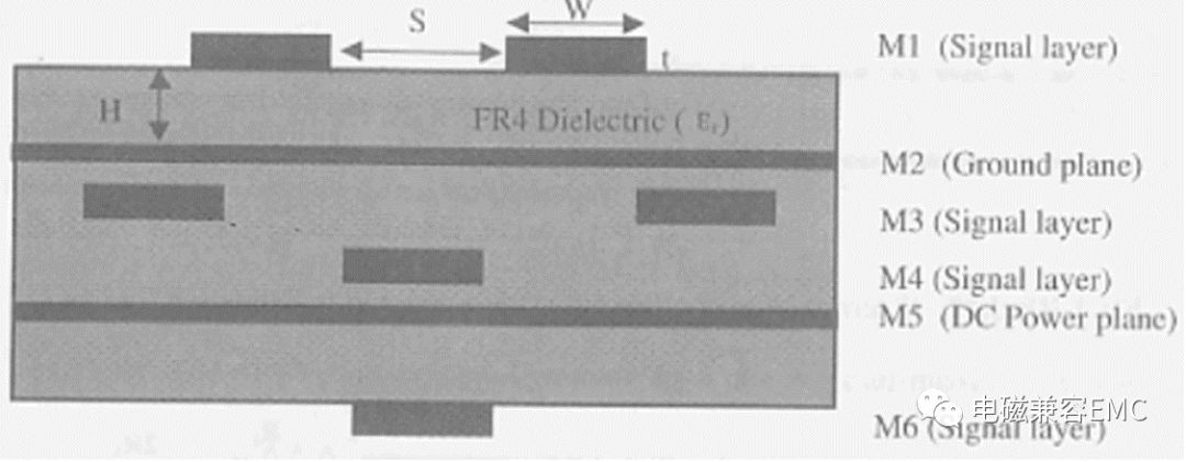
As shown in Figure 1, establish a coupled microstrip line with a port characteristic impedance of 49.93Ω, a line width of 0.25mm, a height of 0.14mm from the GND plane, a dielectric constant of 4.4, and a length of 50mm.

Fig7. Parameters of coupled microstrip line with characteristic impedance of 49.93Ω
Establish a simulation model in the designer according to the previous parameters. The microstrip line 2 is the driver line, the line 1 is the victimline, Vo is the output voltage, NEXT is the near-end crosstalk voltage, and FEXT is the far-end crosstalk voltage.
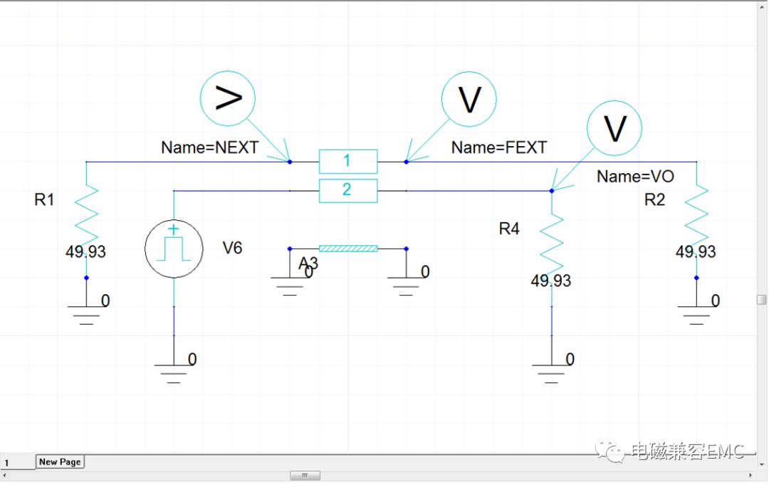
Fig8. Simulation model of coupled microstrip line
The driving signal waveform on the Driver line is a single pulse square wave with a voltage amplitude of 1V, TR=20ps, TF=20ps, and PW=200ps. Figure 3 shows the output waveform of the VO terminal. Several points can be seen from it. First, a voltage drop of 18mV is generated on the transmission line. Secondly, there is a bump of 9.5mV between m3-m4. This is the second reflection of the pulse. The reflections above three times cannot be observed because the amplitude is too small.
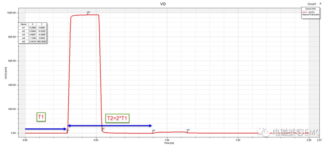
Fig9. VO terminal output waveform
2.2 Delay-time
It can be seen from the results in Figure 3 that the transmission delay of the signal on the coupled microstrip line is about 297ps. Here, Polar is used to verify whether the transmission line delay calculated by different software is consistent. Select the Edge-Coupled Coated Microstrip 1B calculation model, as shown in Figure 4, it can be seen that the Delay-time result is 5.938ps/mm, multiplied by the microstrip line length of 50mm, the total delay is 5.938*50=296.9ps, and The results in Figure 3 are completely consistent.
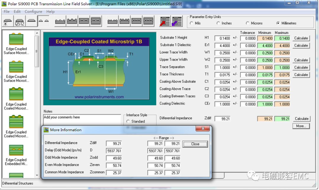
Fig10. Results of impedance and delay calculated by Polar under the same parameters
2.3 Near-end crosstalk NEXT and far-end crosstalk FEXT
It can be seen from Figure 2 that the Victim line and the Driver line also have impedance matching. Figure 5 shows the waveforms received by the near-end and the far-end. Due to the small amplitude, the NEXT curve is multiplied by 25 times, and FEXT is multiplied by 2 times for observation. It can be seen from the result that the near-end crosstalk amplitude is 4mV, and the far-end crosstalk amplitude is 93mV.
Observing the NEXT waveform, it can be seen that the waveform rises from 0s. This is because the near end of the Victim line can receive the noise signal from the Driver line for the first time. During this time, the waveform has not reached the end of the transmission line, and it is considered that the FEXT end is open. , NEXT terminal is short circuit, ICM+ILM is positive, so its voltage amplitude is positive. After 594ps, the NEXT end ushered in the secondary reflection from the FEXT end. At this time, the situation seen from the FEXT end was just the opposite, so the voltage waveform was negative.
Observing the FEXT waveform, it can be seen that the waveform begins to drop at 297ps. At this time, the driver line voltage waveform just begins to rise. At this time, the end of the transmission line is short-circuited, the near end is open, and ICM-ILM is negative, so the received voltage waveform is negative When the time is between 320ps and 520ps, since there is no dV/dt, there is no induced voltage. When the driver line voltage waveform drops, the FEXT terminal receives the opposite dV/dt, so the voltage waveform is positive.
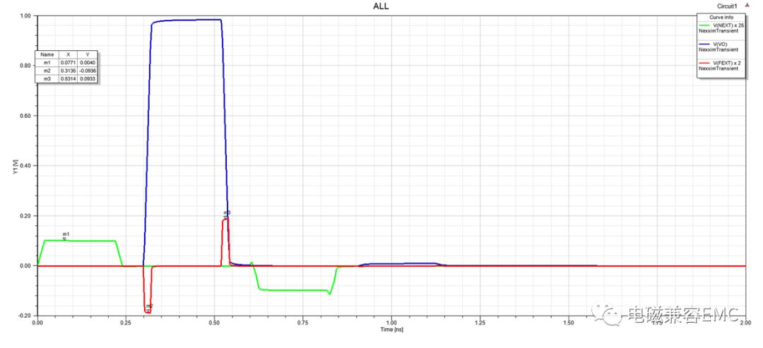
Fig11. Voltage waveforms of NEXT, FEXT and VO
3. The influence of coupling length on crosstalk (multiple crosstalk)
Follow the parameters of the microstrip line in the second section, where the line spacing SP is set to 0.25mm, the length of the microstrip line is set to L, sweepL 10mm~150mm per 10mm, and the three voltage waveforms are viewed.
3.1. Questions?
Usually we think that the width of the far-end crosstalk is equal to the rising and falling edge times of pluse, and both Tr remain unchanged (20ps), and as the coupling length increases, the amplitude of the far-end crosstalk should also increase. However, as can be seen in the figure below, as the parallel traces exceed 50mm, the FEXT size is saturated (476.7mV), and the pluse width increases (>20ps). Why?
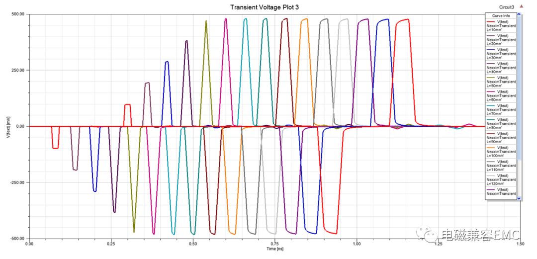
Fig12FEXT terminal voltage waveform
3.2. Reason analysis
In order to find out the reason why the height of the induced pulse of FEXT does not increase at a certain length as the coupling line increases, let us observe the waveform change of Vo as the coupling line length increases. As shown in the figure below, the physical length is above 50mm (including ), Vo's rising/falling starts to change at half the height.
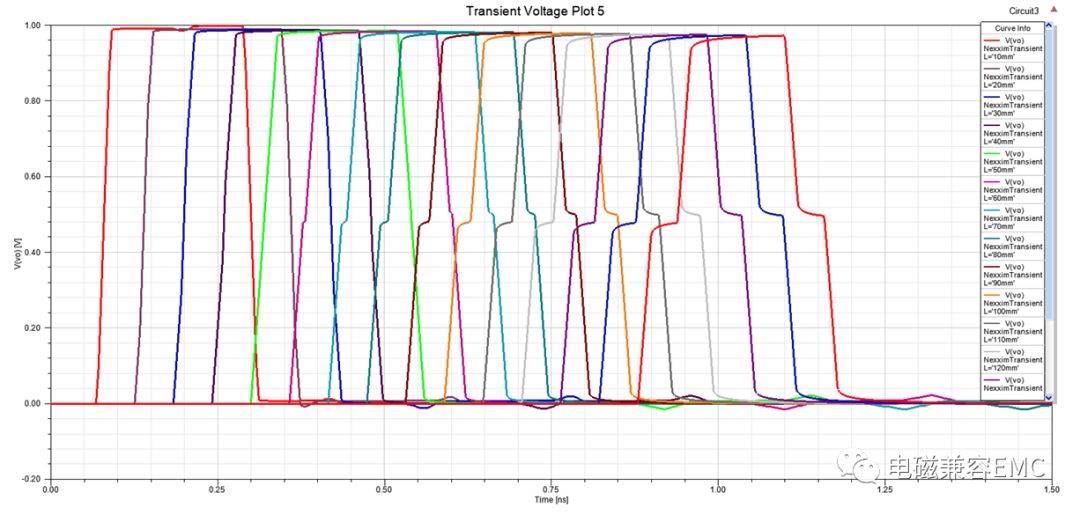
Fig13Vo terminal voltage waveform
Assumption: The FEXT voltage induced by the pulse Vi on the active line on the quiet line returns to affect the pulse signal being transmitted on the original active line, that is, the first FEXT generates secondary coupling (FEXT) to the active line. Then this problem is useless no matter how to adjust the terminal resistance on the active line or quiet line. It is only effective to open the space or thin the stack-up to reduce the crosstalk effect.
So, is it actually the same as the hypothesis? The following figure uses the transmission line model to describe the coupling principle between microstrip lines. We use characteristic impedance Z to replace the complex distributed capacitance and distributed inductance parameters. It can be seen that the common mode impedance of the microstrip line system composed of active line and quiet line It is 50, and the differential mode impedance is about 100. When the length of the microstrip line is infinite, it is considered to be fully coupled. At this time, the circuit model is described by lumped parameters, and the amplitude of the voltage assigned to the end of the quiet line is exactly 1/2 of the active line, which explains why Why the saturation voltage amplitude at the FEXT terminal is about 1/2 of Vo.
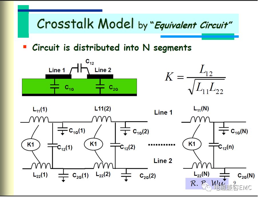
Fig14 The coupled microstrip line model described by the transmission line theory
Because the coupled microstrip line is calculated by the transmission line model, the behavior between them cannot be simply described by lumped parameters. Next, establish a multi-section transmission line model to study the changing process of the signal during transmission. The cross-section parameters of the microstrip line are consistent with the above, the length of the single-section model is 20mm, and the total length is 100mm.
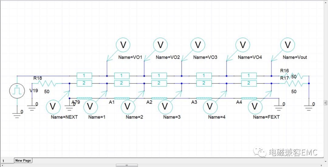
Fig15 signal change process on transmission line
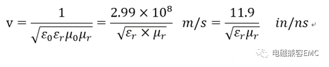
The following figure shows the active line output waveform and quiet line induction waveform of each section. It can be found that as the output waveform is output, as the length increases, the rising edge and falling edge time of the waveform increase, and the horizontal level time is almost unchanged. According to the signal transmission speed in the ideal transmission line (the following formula), the speed is only related to the medium, and has nothing to do with the frequency. So this kind of change shouldn't happen.
The actual lossy transmission line will produce dispersion, so the corresponding high-frequency components in the rising edge and the falling edge will have more attenuation than the low-frequency components as the transmission distance increases. Therefore, as the transmission distance increases, the rising and falling edges will tend to be flat. Because a single rectangular wave pulse signal is used here, when the signal is a continuous pulse, the degraded edge will be superimposed with the subsequent waveform. At this time, the width of the signal remains unchanged, and the superposition will cause more serious oscillations and deteriorate the signal waveform.

Waveform distribution on Fig16 single-section transmission line
If you look closely at Figure 16, you can see that the NEXT waveform is positive while the V1 waveform is negative. Is there a critical value for V1? The answer is no. When the signal starts to enter the active line, a negative voltage will be induced on the quiet line for the first time. As the distance increases, the duration of the negative voltage increases. When the signal is transmitted to the saturation length of the transmission line, the duration of the negative voltage starts to be equal to the time of the rising edge of the signal. Below we verify this conclusion, using SI9000 to calculate the signal delay as 5.745ps/mm, and the delay has an inverse relationship with the transmission speed. So the saturated length of the transmission line is:
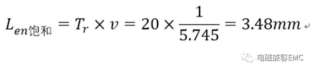
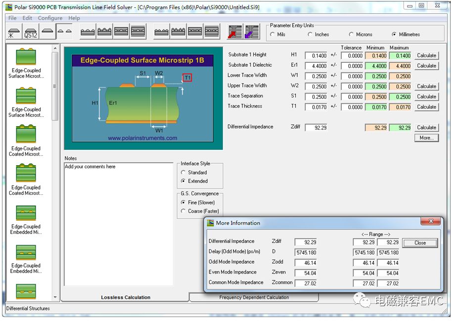
Fig17 Time delay of coupled microstrip line model
When the length of the first section of the transmission line model is adjusted to 3.48mm, the voltage waveform at the V1 terminal is exactly 20ps at the negative level. In the first chapter, it is pointed out that the saturation length is defined as the length corresponding to the near-end crosstalk current reaching a stable value. To the remote end, also refers to the length of the remote end voltage that is equal to the rising edge time and no longer increases.
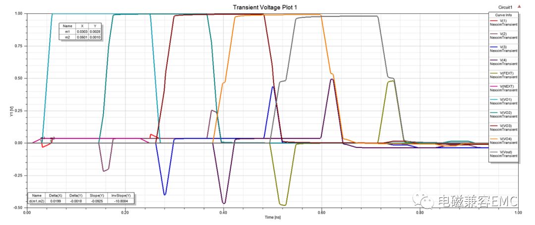
Fig18 Coupling voltage waveform at saturation length position
3.3, the situation of secondary reflection
Looking at the waveform of the NEXT terminal in Section 3.1, it can be seen that only when the transmission line length is 10mm, the voltage waveform width is less than 20mm or more. It can be seen from Section 3.2 that the transmission line delay is 5.745ps/mm, and when the length is 10mm, the coupling waveform time length is 57.45ps. In the result, the time corresponding to m1~m2 is 117ps. Why?
As the length of the transmission line increases, the waveform returned by the secondary reflection appears to be significantly collapsed. The cause of this situation is the same as the FEXT situation in section 3.2.
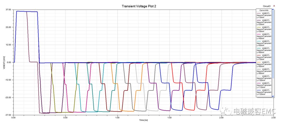
Fig19 NEXT terminal voltage waveform changes with length
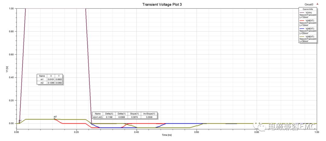
Fig20NEXT terminal voltage waveform and active line input waveform
3.4, active line and quiet line parameter adjustment
On the basis of 3.1, the same simulation parameters were run again, but the distance between the active line and the quiet line was changed from 0.25mm to 0.75mm. We found that both NEXT and FEXT became smaller, and when the physical length increased to 160mm, FEXT It starts to saturate, that is, the parallel coupling length of 160mm, the first FEXT induced voltage will affect the pulse signal being transmitted on the original active line.
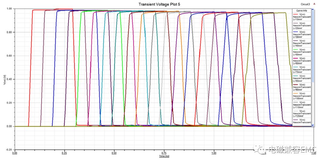
Fig21 The output voltage waveform after the distance is opened
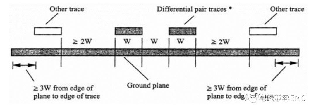
4. The influence of pitch change on crosstalk (origin of 3W principle)
In the second section, the default spacing S of the simulation model is 1mm, and the line width W is 0.25mm. Here we adjust the line spacing S to a multiple of 0.25mm. The value of S is increased from 1W to 5W. Check the NEXT and The changing law of FEXT crosstalk amplitude. It can be seen from Fig. 6 and Fig. 7 and Fig. 8 that as the spacing increases, the amplitude of the crosstalk voltage at the NEXT and FEXT terminals first decreases rapidly, and as S continues to increase, the downward trend slows down.
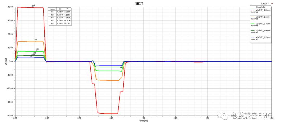
Fig22. NEXT end crosstalk amplitude changes with S
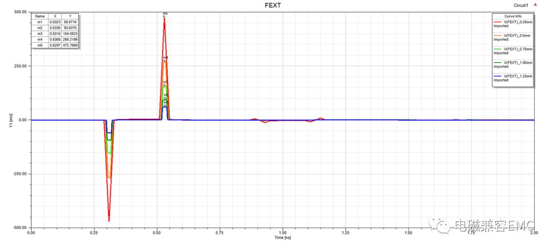
Fig23. The crosstalk amplitude of FEXT end varies with S
The crosstalk 3W rule as we know it generally refers to: It is safe to maintain a 3W spacing for a transmission line with a characteristic impedance of 50Ω. For the case where the characteristic impedance is higher than 50Ω, the spacing of 3W is often not enough.
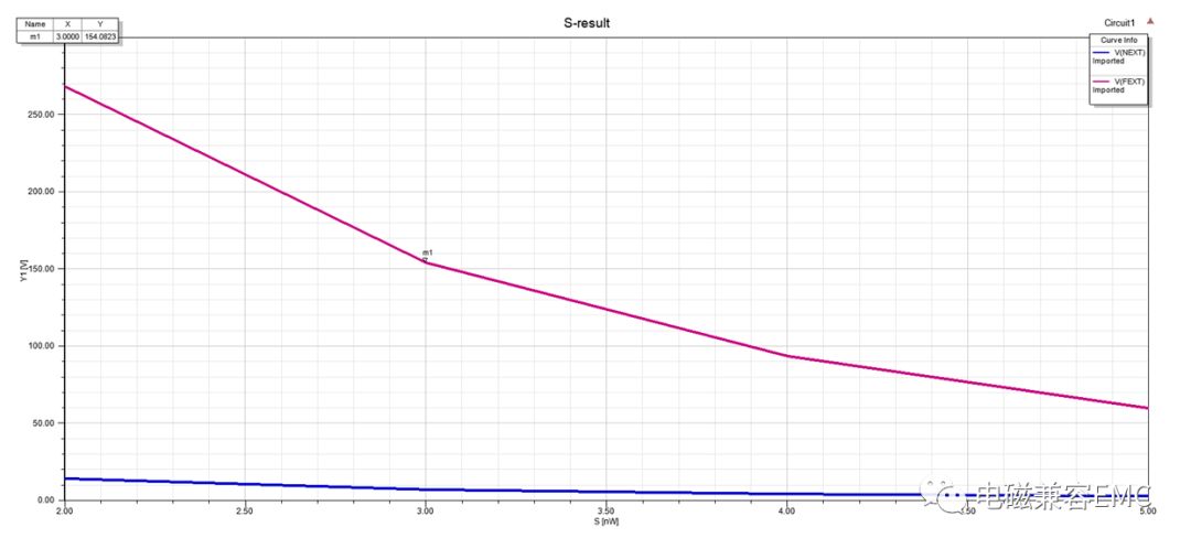
Fig24. Victim line increases with S, the trend of crosstalk voltage received at both ends
The following is Montrose's description of the 3W principle in the book "Printed Circuit Board Design Techniques for EMC Compliance"
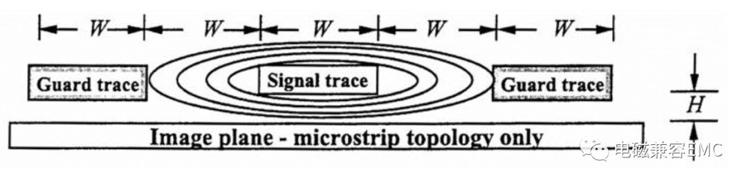
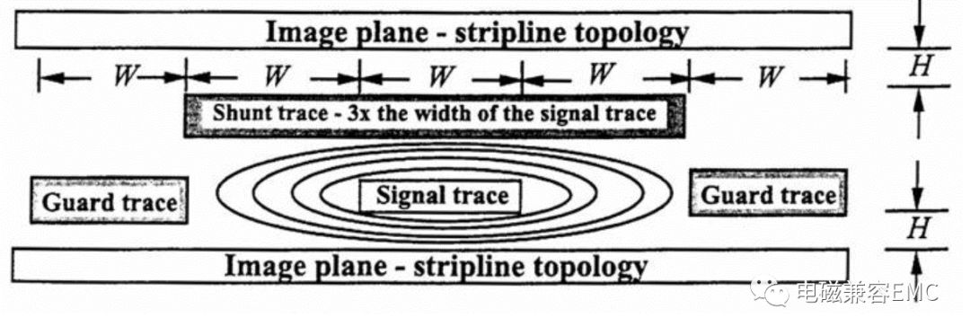
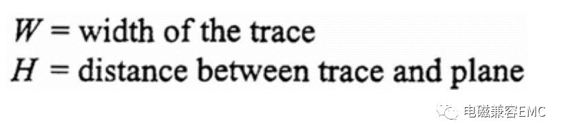
5. The influence of the protective ground wire on crosstalk (Guard Trace Effect)
From the perspective of PCB design, in addition to keeping a certain distance between sensitive signal lines, a protective ground line is often considered during the design to further protect the wiring from being affected. The role of the protective line is mainly to introduce a low impedance boundary, and lead the power line emitted from the signal line to the ground loop. Next, use ANSYS to simulate the protective line to see its impact on crosstalk.
Fig25.With/withoutguard trace
5.1 The influence of the protective ground wire under the fixed line width
The following figure has a trace width of 7 mils, a trace distance of 7 mils (line edge to edge), a via diameter of 5 mils, a ground guard trace line width of 10 mils, a line length of 50 mm, and a board thickness of 1.6 mm. One wire is accompanied by a ground wire, and four wires are accompanied by a ground wire.
5.1.1 Two wires interspersed with a ground wire
In the model shown in Figure 26, the trace numbers are T01~T09 from top to bottom. The left side of each trace is the L port and the right side is the R port. Figure 27 shows the S21 parameters of each trace.
Fig26. Two wires interspersed with a ground wire
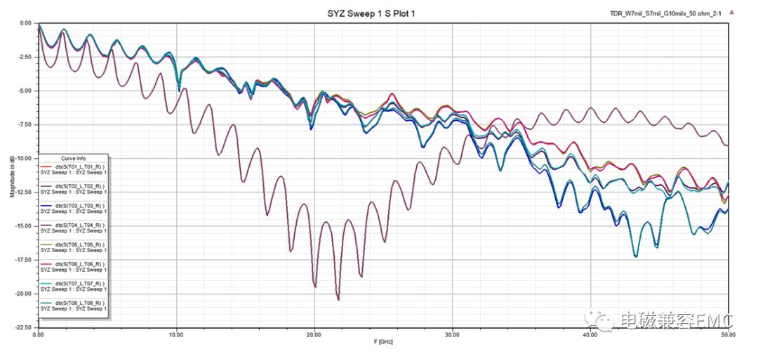
Fig27. S-parameters for S21
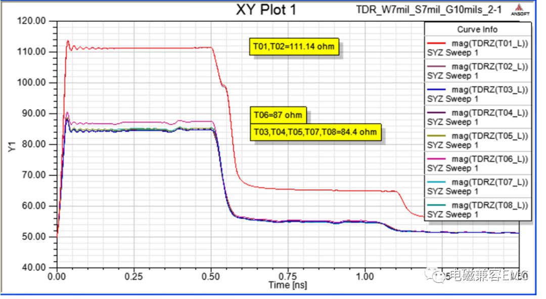
Fig28.TDR results
T03~T08 have the same structure, and S21 should be similar. From the simulation results of this example, the accuracy of SIwave is about 25GHz, and the official statement given by Ansoft at that time is that SIwave is suitable for DC~50GHz.
5.1.2 Four wires interspersed with a ground wire
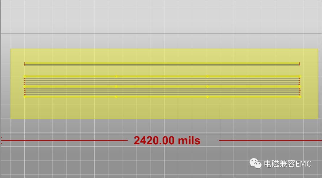
Fig29. Four wires interspersed with a ground wire
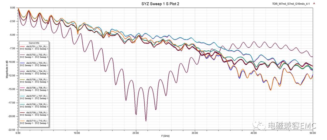
Fig30.S-parameters for S21
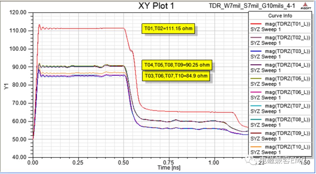
Fig31.TDR results
As long as there is an accompanying ground wire, whether it is two wires interspersed with a ground wire, or four wires interspersed with a ground wire, the performance of S21 is almost the same (1dB) within 20GHz. But if there is no accompanying ground wire, the difference can be seen at 1GHz, and the S-parameter characteristics are much worse.
Without the signal accompanying the ground wire, the characteristic impedance is significantly larger (T01, T02=111Ω), and as long as there is an accompanying ground wire, whether it is two wires interspersed with a ground wire, or four wires interspersed with a ground wire, the characteristic impedance will be at Between 84~90Ω. The ground wire here is 10mil, which is not very wide, and the via pitch is 17mm.
5.2 The influence of the line width of the protective ground wire
As shown in the figure below, a microstrip line model with a characteristic impedance of 50Ω is established. The line width is 14mil, the dielectric thickness is 8mil, the dielectric constant is 4.4, the trace length is 1975mil, and there is a variable width accompanying ground wire between the two signal lines. , The ground wire is grounded through both ends. Check the change of the ground wire width and the change of the noise waveform on the victim wire. The initial width of the ground wire is 5 mils, and the width is increased by 2 mils each time.
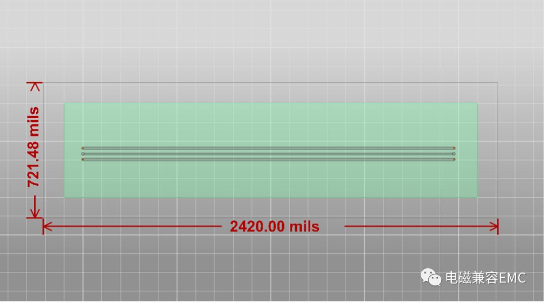
Fig32. Accompanying ground between two traces
6. The impact of protective vias on crosstalk
The design of vias in the PCB is a link that most people tend to ignore. The design of vias directly affects many parameters. For the power plane vias, it will directly affect the voltage drop of the power supply network, the distribution parameters, and change the resonance characteristics of the power supply network; In the signal part, the introduction of vias will affect the integrity of the signal; when used as a connection between the various layers of the GND on the board, the via directly affects the distribution of the GND plane noise current, which is related to the size of the signal loop area.
Lu Junlang and others mentioned the following points in the analysis of the via effect in the article "The Via's Effects on PCB Traces":
For the same via, the capacitance effect of the mathematical via model is larger than that of the actual via measurement, and the capacitance effect of the via is mainly the capacitance effect compared with the inductance effect.
The first via on the trace has the greatest impact on impedance discontinuity. As the number of vias increases, the via capacitance effect does not increase significantly. This is because vias and transmission lines will bring high-frequency signal loss, so the effect measured by the analysis instrument is also decreasing.
The thinner the PCB, the smaller the via capacitance effect (and the smaller the inductance effect).
The capacitance effect of the via has little difference between the microstrip line and the strip line.
When the line width is greater than or equal to the diameter of the via, the impedance discontinuity formed by the via almost disappears, and the via effect at this time is very small.
When using vias to change layers to different layers, if the same ground plane can be referenced, the capacitance effect of the vias is smaller (the inductance effect will also be smaller), and the impedance discontinuity caused by the layer change is lighter.
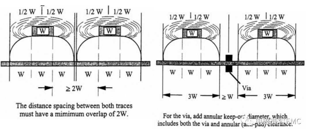
Li Liping proposed in the article "FDTD Analysis of Protection Lines to Reduce Crosstalk Between Microstrip Lines", as long as: (1) Add a protection line with ground vias and make the via spacing smaller than the signal at Tr/2 (Tr: transmission Signal rise time) the transmission distance within the time period; (2) Under the premise of satisfying the line spacing and wiring rules, appropriately widen the protection line while maintaining between two of the three lines (protection line and two microstrip lines) If the center distance is constant, the far-end and near-end crosstalk between the lines can be effectively reduced.
According to the model in Section 5.2, place a GND via every 250 mils on the middle protective GND trace, as shown in the figure below.
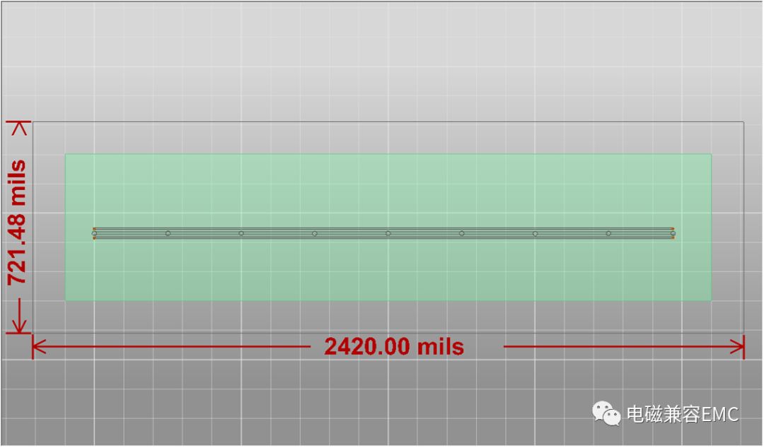
Fig33. Protective ground wire with GND hole
The single-line impedance calculated by SI9000 is 144.22Ω. Because of the GND, the actual TDR impedance calculated by siwave is 110.19Ω. The line delay is 140.247ps/in. In order to satisfy the hole spacing to be less than Tr/2, RT must be greater than 70ps.
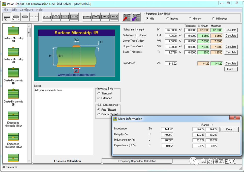
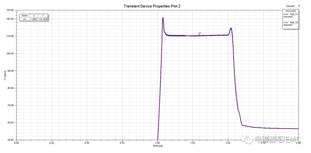
Fig34. Trace characteristic impedance and time delay
We set the RT time to 40ps, 70ps, and 100ps respectively, and check the changes in the amplitude of the crosstalk voltage on the victim line, as shown in the figure below. It can be seen that the change of the rising edge time has little effect on the near-end crosstalk level, and mainly affects the far-end crosstalk level. The definition of Tr/2 greater than the hole spacing is in the design requirements for far-end crosstalk protection. When the Tr time is constant, the same conclusion can be drawn when the via pitch is changed, and interested readers can calculate it by themselves.
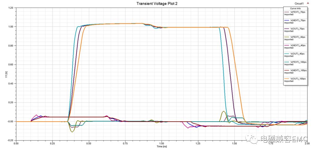
Fig35. Crosstalk voltage waveform under different Tr
Note: There will also be crosstalk between high-speed signal vias. For a thicker PCB, taking a 3mm single board as an example, the length of a via in the thickness direction of the PCB can reach nearly 118mil. If the fan-out via hole pitch on the PCB is small, such as a BGA packaged IC, the fan-out via hole pitch is only tens of mils. At this time, the vertical parallel distance between the vias is greater than the horizontal distance, and the problem of high-speed signal cross-space crosstalk needs to be considered. High-speed PCB design should minimize the length of the via root as much as possible to reduce the impact on the signal. Readers who are interested can go to the TI forum to view the article "Analysis of Crosstalk Between High-Speed ​​Differential Vias".
7. Minimization of Crosstalk
7.1 Wu Ruibei's design method
In the Crosstalk_App article, the centralized design methods to reduce crosstalk are listed as follows:
• Under the premise of the wiring permit, increase S and reduce H as much as possible;
• Critical signal lines, such as system clock, adopt differential wiring;
• Use orthogonal wiring between layers with significant coupling;
• If possible, use stripline instead of microstrip line as much as possible;
• Control the parallel length between signal lines to a minimum;
• Reduce the congestion of wiring between components on the PCB board;
• Use slower edge rates with caution.
• Use genius layout design, say Tx-line interpose.
7.2 Views of Y.-S. Cheng, W.-D. Guo, etc.
They proposed in the article "Enhanced microstrip guard trace for ringing noise suppression using a dielectric superstrate" that by adjusting the thickness and dielectric constant of the solder mask, the effect of suppressing crosstalk can be achieved. Referring to the formula of the amplitude of the far-end crosstalk in Fig. 6, it can be found that when the dielectric constant and thickness of the solder mask reach a certain value, the far-end crosstalk will disappear.
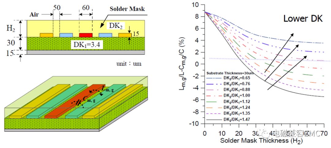
Fig36.Novel Guard Trace Design
8. ANSYS crosstalk check module
The CrosstalkScan crosstalk analysis module is provided in ANSYS SIwave, with time domain and frequency domain options respectively, which can quickly analyze crosstalk on single/differential lines. In Figure 33, a PCB is taken as an example. The arrow position in the figure is U1's crystal oscillator X2, clock The trace XTALIN and the signal line A_HSYNC_DAC1 have a long parallel trace, and the impact of the clock trace on the signal line needs to be evaluated.
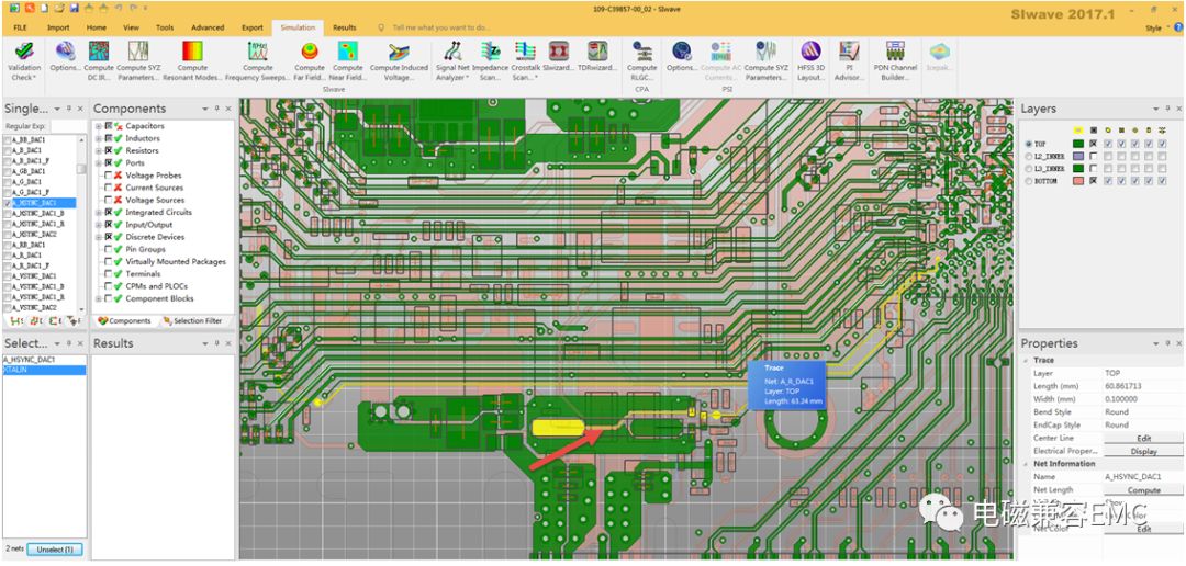
Fig37.SIwave simulates a PCB example
8.1 Parameter setting
Checking the chip manual and schematic diagram, you can know that the A_HSYNC_DAC1 signal is an RGB output signal, the level is 1.8V, and the rate is 400MHz, and the XTALIN signal level is also 1.8V, and the rate is 27MHz. The rise time of the DAC signal in the check specification is 0.58ns~1.7ns, which is 1ns, the DAC signal is in the form of check points, the differential impedance is 75R, and the impedance to ground is 37.5R. XTALIN signal rise time is 4ns under 15pF load, here is 12pF, set it to 3ns.
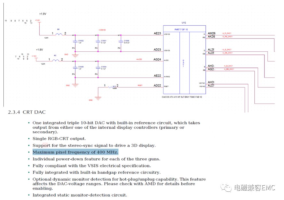
Fig38. Signal parameters
Before simulation, adjust the accuracy to a suitable level, adjust the crosstalk convergence accuracy to -60db, increase the solution frequency to 20GHz, and then select Time domain simulation, fill in the corresponding parameters of the signal into the signal definition of the two traces, and select Launch the simulation.
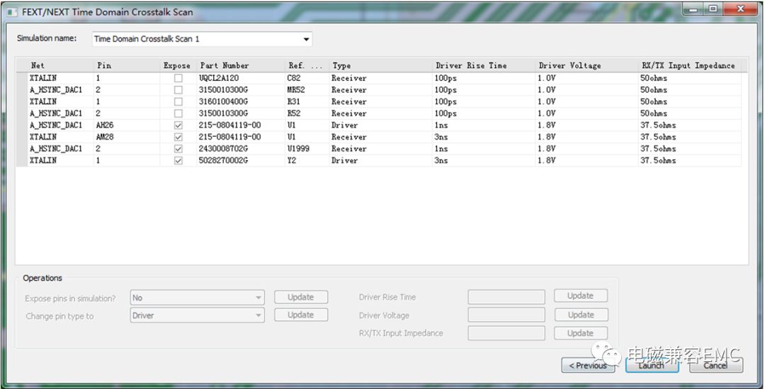
Fig39. Parameter setting
After less than half a minute, the simulation ends. Check the voltage waveforms respectively coupled to the FEXTt and NEXT terminals. As shown in the figure below, it can be seen from the results that the NEXT coupling noise generated by A_HSYNC_DAC1 on the XTALIN line is the highest, about 0.001V. Generally, the safety threshold of the crosstalk level in signal traces is about 5% of the signal level, so these two traces are considered OK on the wiring.
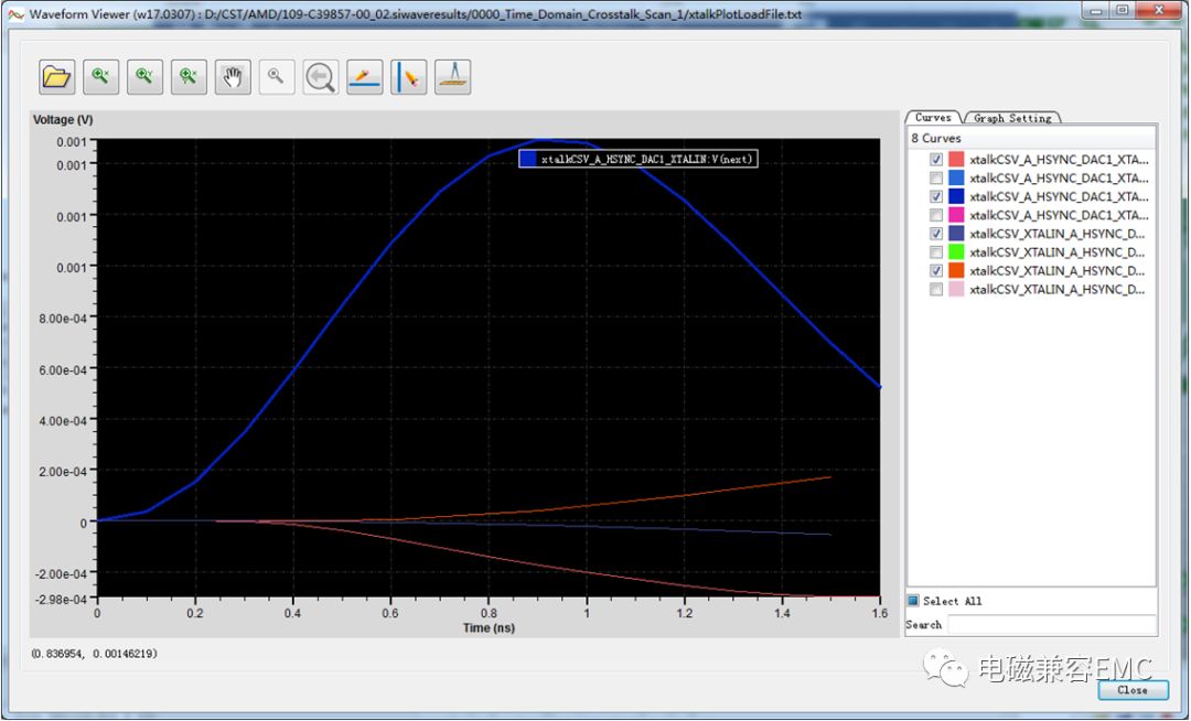
Fig40.crosstalkresult
The results not only provide the waveform of the coupling on the signal line, but also have the peak bar graph and the FEXT/NEXT time domain coupling peak position. From the coupling structure diagram, you can intuitively see the more severely coupled parts of the trace. It can be seen from the figure below that the local coupling in parallel routing is more serious. When the result exceeds the safety threshold, it needs to be processed.
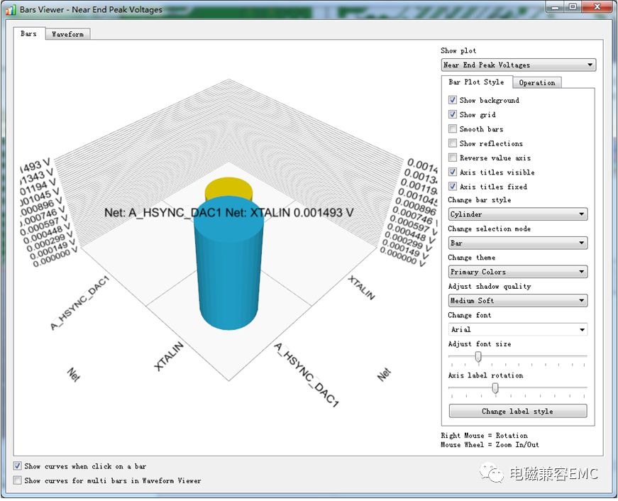
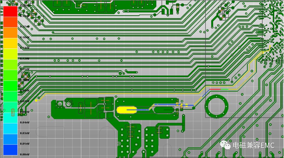
Fig41.Peak Voltage and Time Domain Crosstalk Max Voltages results
Because the overall layout of the wiring has been determined, here we choose to add a part of the accompanying GND wiring between the lines. When the simulation is performed again after optimization, it can be seen that the level at the original position has dropped.

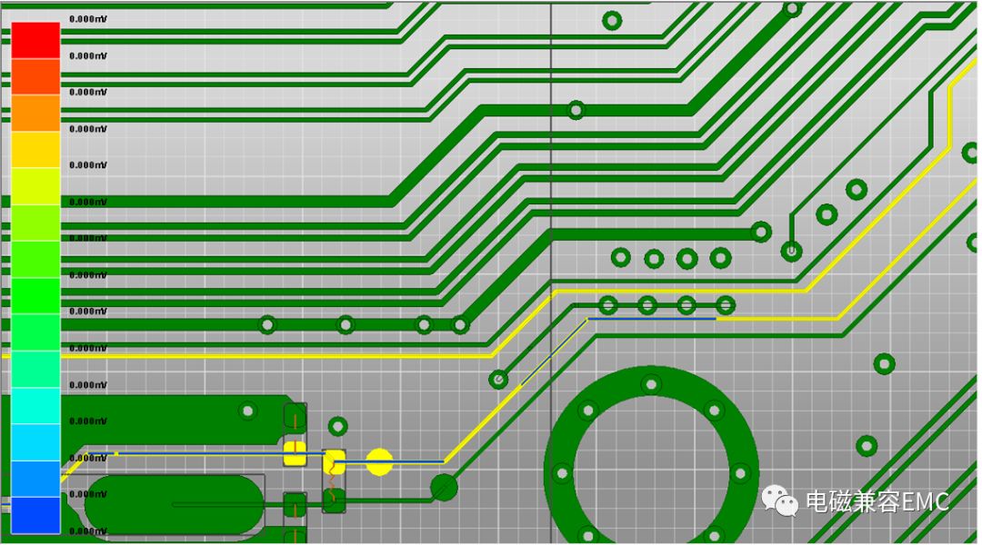
Fig42.Peak Voltage and Time Domain Crosstalk Max Voltages results
8.2 Optimization
The S-parameter model is used to simulate time domain crosstalk. Because the Time Domain Crosstalk function is not based on accurate S-parameter solution, in order to clearly understand the comparison before and after optimization, the S-parameter model is used here to create the crosstalk circuit model in the circuit design. The crosstalk waveform before and after optimization is shown in the figure below (_2 is initial, _1 is after optimization). It can be seen that after the optimization, the positive voltage increases and the negative voltage decreases, and the overall level is flat, but there is no obvious change after optimization. Can it be considered that the protection line has no effect?
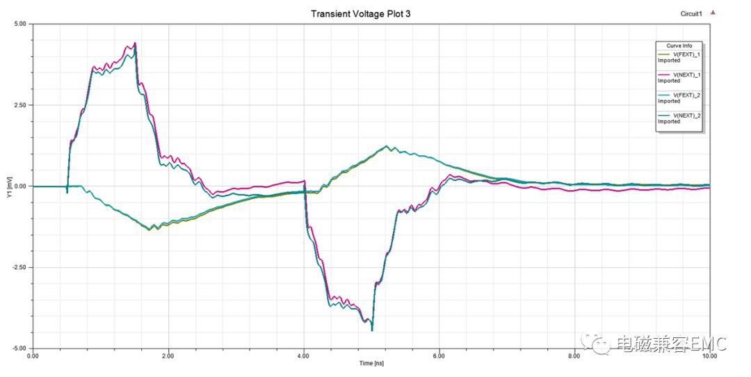
Fig43.Results of crosstalk
Note: The reason why the comparison is not obvious here is that the relationship between the protective ground hole and the rising edge of the signal is mentioned in Chapter 6. The signal Tr in the actual circuit is unchanged, and in most cases it is not allowed to add a capacitor to increase the Tr time. In this case, it is only possible to ensure the line spacing is greater than 3W.
9. Crosstalk between cables
Cable design In EMC design, crosstalk between cables is often ignored. However, the actual situation is that a considerable part of the design defects of products come from the crosstalk between cables. Such problems mostly come from the strict requirements of military, medical, automotive and other standards, complex structures, and many interconnection cable products.
The crosstalk between adjacent wires can be caused by electric field coupling caused by mutual capacitance or magnetic field coupling caused by mutual inductance. The third form of coupling is caused by common impedance.
When encountering data transmission errors in the cable interface, it may not necessarily be caused by crosstalk. There is also a reflection that may be caused by the impedance mismatch between the line and the load. The latter is often mistaken for crosstalk. (About reflection will be summarized in detail below)
So, when an EMI problem occurs, how to determine whether it is caused by crosstalk? A practical method is to separate the source of interference from the sensitive wires. If this method is not easy to implement, then reducing the rising edge of the interference source signal or reducing the frequency may be another feasible method. When intermittent EMI is generated and crosstalk is suspected, it can be confirmed by increasing the amplitude, frequency, and speed of the interference source signal or injecting another noise source through a transformer or capacitor. At this time, if the EMI trend is increasing, it may have been found that there is a source of crosstalk.
When crosstalk has occurred between PCB lines and adjacent wires, it is first necessary to determine whether the coupling is mainly electric field coupling (capacitive) or magnetic field coupling (inductive), because different coupling methods determine different processing methods. David A. Weston proposed a simple and effective method in "Electromagnetic Compatibility Principles and Applications". The author uses the characteristic impedance between the interference source and the sensitive circuit and the impedance between the sensitive circuit and the ground wire in the crosstalk estimation. The criteria are as follows:
When the product of the interference source and the impedance of the sensitive circuit is less than 300²Ω, it is mainly magnetic field coupling;
When the impedance product is greater than 1000²Ω, it is mainly electric field coupling;
When the impedance product is between 300²Ω and 1000²Ω, whether the magnetic or electric field coupling can play a major role depends on the geometrical size and frequency of the circuit.
Seeing this, it is not difficult for a careful reader to find that magnetic field coupling or electric field coupling occurs in specific circuits respectively. The power supply part of the product is often low resistance (magnetic field coupling), the signal is often high resistance (electric field coupling), and the coupling between the power supply and the signal is somewhere in between.
For a single line with a diameter of d and a height of h from the ground plane, as shown in the following figure:
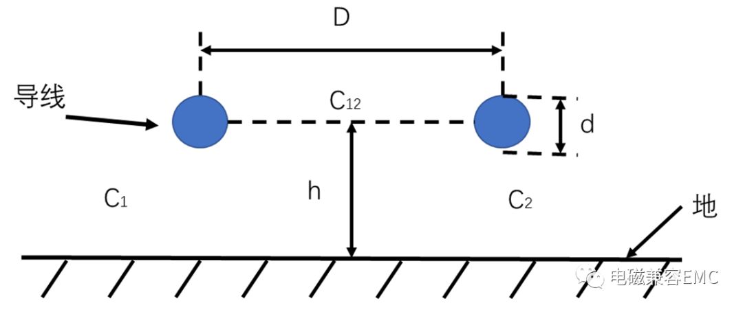
Fig44.Cable model
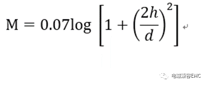
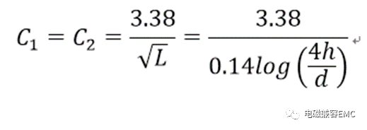
The wire inductance L (Uh/ft) is:

The mutual inductance M (Uh/ft) between the two wires is:
The line-to-ground capacitance is:
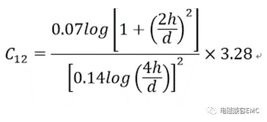
The line-to-line capacitance (mutual capacitance) is:
The crosstalk model between parallel double lines is shown in the figure below:
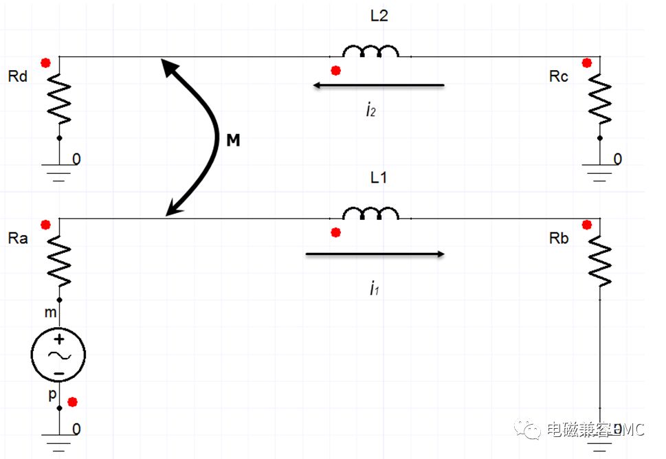
Fig45. Cable coupling model
The voltage amplitude at both ends of the disturbed load Rd can be calculated by the following formula:
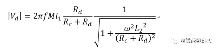
It can be seen from the formula that when the distance h between the wire harness and the ground decreases, the wire inductance L and the mutual inductance M between the wires decrease at the same time. When h decreases to 1/10 of the previous value, the self-inductance L decreases by 0.14 (uH/ft) (according to The maximum distance h is 50mm and d is calculated as 2mm. Under normal circumstances, the self-inductance of the internal wiring harness of the product is about 0.2 (uH/ft). The trend of mutual inductance reduction varies with the ratio of h to spacing D. It can be seen from the calculation formula of Vd that when the disturbed line is high resistance, or the disturbed line is low resistance, the crosstalk increases. The following uses CST cable studio tool to describe this change to readers.
9.1. Crosstalk between single lines
9.1.1 Establish a cable model
Choose a single wire with a wire diameter of 0.2mm, the length is 100mm, the line spacing is 5mm, the line and GND spacing is 5mm, the signal Tr of the driver line is 0.1ns, the Tf is 0.1ns, the period is 2ns, the 50% duty cycle, and the amplitude is 1V.
Fig46. Coupling line model
Check the near-end and far-end waveforms on the victim line. As shown in the figure below, the voltage amplitude on the victim line is about 2% of the level of the victim line. Even if the signal level of the disturbing wire is increased to 3.3V or 5V (most signal levels), the noise level of the disturbed wire is acceptable.
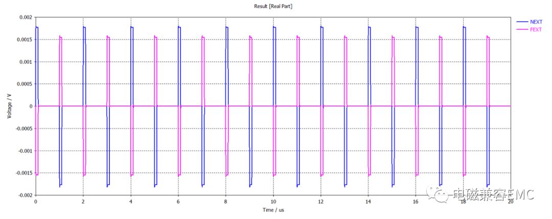
Fig47. Noise voltage waveform of the victim wire (ground impedance 50R)
9.1.2 Does the wiring harness design necessarily meet the demand?
So, does this kind of wiring harness design meet the demand in practice? The answer is no, because the impedance of the signal line in the actual circuit is often high impedance, especially the impedance of the sampling signal line bundle is usually above 1,000Ω. When the impedance of the victim line increases to 1MΩ, the noise level on the line will increase to a level that cannot be achieved. The level of acceptance. In the results shown in the figure below, the FEXT and NEXT levels are increased to 0.18V. In real products, the wiring harness is often tied up (D is reduced) and there are longer wiring (for example, the EMC test requires the wiring harness length to be about 2 meters). These conditions will increase the noise level of the disturbed line, especially when doing EMS immunity test, if the signal line is not protected by filtering and other protection, the product is very easy to be disturbed. Comparing the upper and lower figures, it can be seen that FEXT and NEXT have changed from the initial phase phase to the phase phase. Why is this? This question is left to the reader to think about.
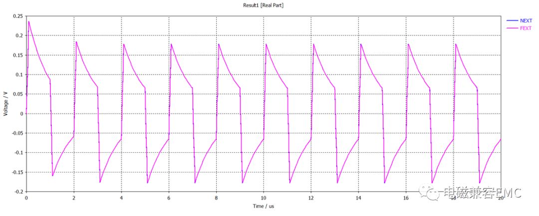
Fig48. Noise voltage waveform of the victim wire (ground impedance 1MR)
When the overall impedance of the signal line changes, the relationship between its noise level and the impedance of the signal line is shown in the figure below. It can be seen that controlling the signal line impedance to a small level can effectively reduce the crosstalk level amplitude. It can also be seen that the effect of using capacitor decoupling on the signal line is the best, far better than inductance (the reason will be discussed in the filtering article).

Fg49. The noise level of the disturbed wire changes with the ground impedance
9.1.3 "3W principle" in cables
In fact, people usually only pay attention to the signal routing in the upper part of the PCB in product design, and ignore the wiring harness design. The wiring harness is actually an extension of the PCB, which also requires attention in the layout. When increasing the distance D of the wiring harness, observe the change of the crosstalk amplitude, as shown in the figure below, when the distance D is increased to 15mm (3 times h), the noise level decreases gradually. Therefore, for sensitive signals, the wiring of the wiring harness needs to be strictly controlled, and independent wiring must be used when necessary.
Note: Change the distance between the wire and GND h, and the obtained trend is the same.
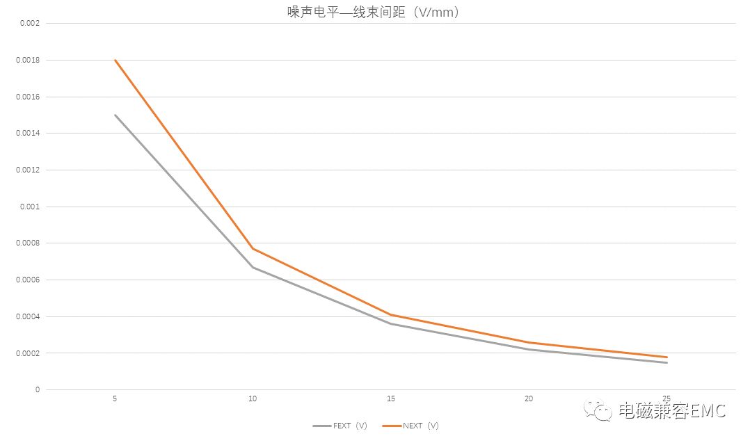
Fig50. The noise level of the disturbed line varies with the line spacing
9.1.4 Analysis of the influence of GNS distance
It can be seen from the previous formula that reducing the distance between the wiring harness and the GND plane can reduce the amplitude of crosstalk between the wiring harnesses. Here, the software is used to calculate the change of the crosstalk amplitude with the change of the GND spacing h. As can be seen from the results in the figure below, as the distance between the wiring harness and GND increases, the crosstalk amplitude increases. Within the allowable distance range of the design, the overall trend is approximately a linear increase. In other words, when h is reduced by one time, the amplitude of the noise level on the victim line is reduced by 3dB.
Note: Changing the distance between the wires leads to the same trend.
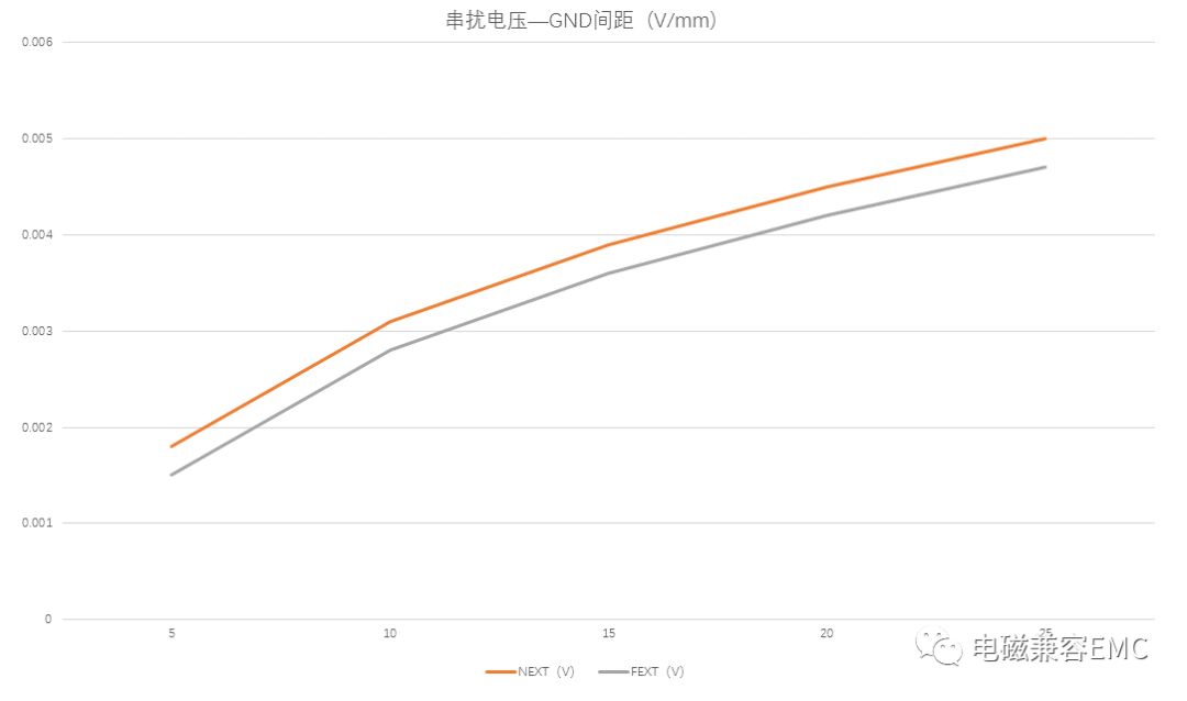
Fig51. The noise level of the disturbed line varies with the GND spacing
9.2 Crosstalk between harnesses of different specifications
Most product designs often use different specifications of wire harnesses, including single wire, twisted pair, coaxial wire, shielded twisted pair, and even multi-harness shielded wire. So, what are the protection capabilities of these wiring harnesses against crosstalk? The following is an analysis of this problem.
Use CST cable studio to establish single wire, twisted pair, coaxial and shielded twisted pair models, as shown in the figure below.
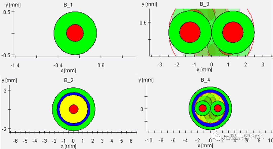
Fig52. Cross-section view of simulation harness
The wiring harness length is also set to 100mm, the wiring harness spacing is 5mm, and the distance from the GND plane is 5mm. The wiring harness is arranged as a single wire (single wire) at the bottom, and a single wire, twisted pair, coaxial wire, and shielded twisted pair every 5mm upwards. The model after extracting the S parameters is shown in the figure below.
Note: here twisted pair refers to differential twisted pair.
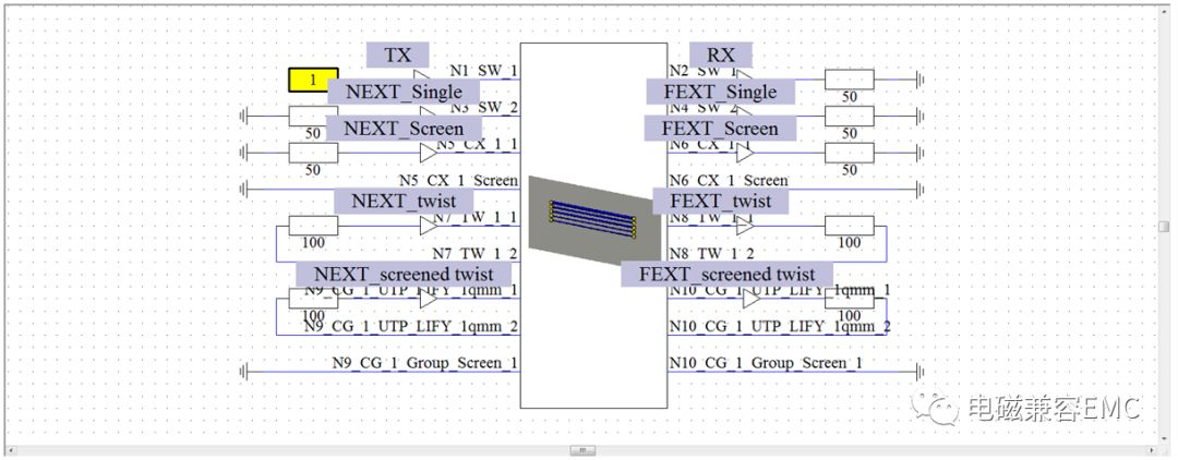
Fig53. Wiring harness topology diagram
After the simulation is completed, check the amplitude of the noise voltage on each wiring harness and select the FEXT result. You can see that the noise voltage waveforms on the adjacent wiring harnesses are as follows (the value difference is too large, and compare them separately). It can be seen that the single wire and the twisted pair wire The crosstalk noise is much higher than that of coaxial cables and shielded twisted-pair cables, and the noise level of twisted-pair cables is the highest. Most engineers twist the wiring harness in the product design. It can be seen that twisting is not always advantageous. It will not reduce the common mode noise on the wiring harness, but will increase the noise amplitude. According to the reciprocity theorem, the wiring harness that is easy to couple noise is also easy to interfere with other wiring harnesses. Therefore, for those wiring harnesses that have to be twisted due to design needs (such as unshielded network cables, video cables, CAN cables, etc.), they need to be kept with other wiring harnesses. Distance (or direct shielding), the specific distance can refer to the results of Section 9.1.
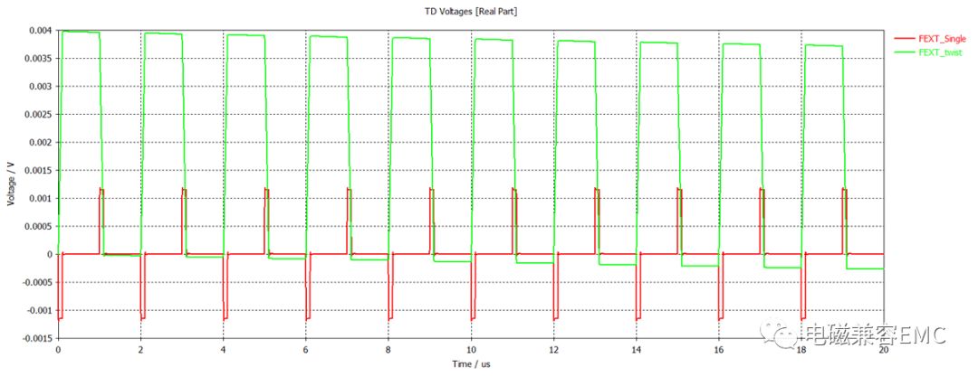
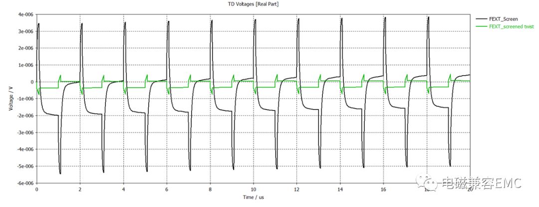
Fig54. Far-end crosstalk voltage waveforms on different wiring harnesses
In practice, the working signal in the differential line such as the network cable, video line, CAN line, etc. is in differential mode, so we need to evaluate the crosstalk on the differential mode signal instead of common mode. After changing the test probe, we can see that the differential mode noise amplitude on the twisted pair cable is abnormally small, so small that it can only be viewed separately.
Note: The twisted-pair shielded wire in the above figure results in common mode noise. If it is changed to differential mode noise, its amplitude will be the smallest.
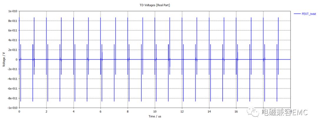
Fig55. Differential mode noise voltage waveform of twisted-pair shielded wire
So, for those who twist the single wire, will there be any difference? The results in the figure below can intuitively find that after the single wire is twisted, the noise level is reduced by about 30 times compared with the case without twisting (assuming The single-wire input impedance is 10kΩ).
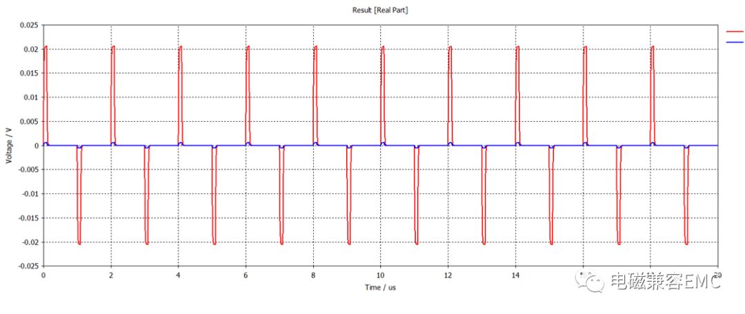
Fig56. Voltage waveform change of near-end crosstalk noise before and after single-wire twisted pair
9.3. Crosstalk between cables of different specifications in the same harness
In actual product design, we will encounter various types of wiring harnesses, such as CAT5E_STP (Cat5e shielded cable), CAT5E_UTP (Cat5e unshielded cable), USBr3 (USB3.0 high-speed data cable), etc., and wiring harness manufacturers Will meet customer requirements for wiring harness design.那么,如æ¤å¤šç§ç±»çš„线æŸåº”该如何去设计呢?下图最åŽä¸€å¼ 为自定义线æŸï¼Œä¸Ž9.2节相åŒï¼Œä¸€æ ¹å¤§çš„å±è”½çº¿æŸå†…包å«äº†å•çº¿ã€åŒç»žã€åŒè½´ã€å±è”½åŒç»žç‰å¸¸è§çš„线型。
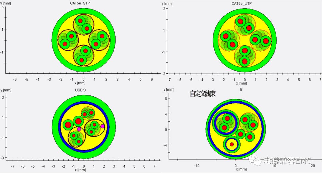
Fig57.ä¸åŒè§„æ ¼çº¿æŸæ¨ªæˆªé¢
当在上图å³ä¸‹è§’çš„å•çº¿ä¸æ³¨å…¥å™ªå£°ï¼Œæˆ‘们观察其它åŒåœ¨ä¸€æ ¹çº¿ç¼†å†…的线æŸä¸Šå™ªå£°æƒ…况,以æ¤æ¥åˆ¤æ–è¿™æ¡çº¿æŸæ˜¯å¦ç¬¦åˆè¦æ±‚。首先我们查看其它线æŸä¸Šçš„共模和åŒç»žçº¿ï¼ˆå·®åˆ†ï¼‰ä¸Šçš„差模噪声。å¯ä»¥æ˜Žæ˜¾çœ‹å‡ºåŒç»žçº¿ä¸Šå·®æ¨¡å™ªå£°æ˜¯æœ€é«˜çš„,å•çº¿æ¬¡ä¹‹ï¼Œå™ªå£°æœ€å°çš„是å±è”½åŒç»žçº¿ã€‚
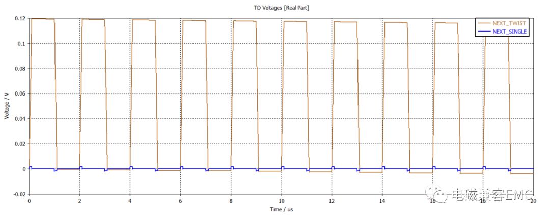
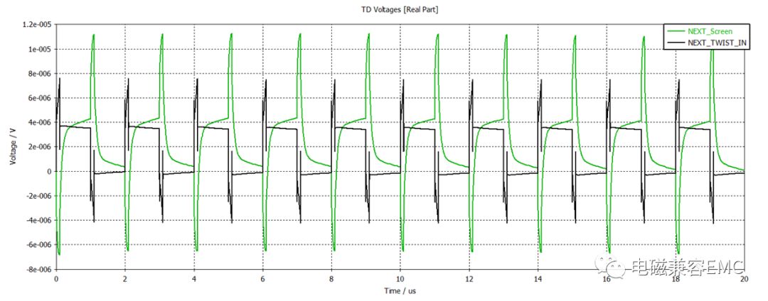
Fig58.线æŸå†…ä¸åŒçº¿é—´è¿‘端串扰电压波形
当åŒç»žçº¿ä¸ºå•çº¿è€Œéžå·®åˆ†å½¢å¼ï¼Œæˆ‘们关注的噪声模å¼è½¬æ¢ä¸ºå…±æ¨¡ï¼Œå†æ¥æŸ¥çœ‹çº¿æŸä¸Šå™ªå£°æƒ…况我们会å‘现,åŒç»žå•çº¿è¦æ¯”å•çº¿ä¸Šå™ªå£°å¹…值低一å€è¿˜å¤šã€‚而åŒè½´å’Œå±è”½åŒç»žçº¿ä¼¼ä¹Žæ²¡æœ‰ä»€ä¹ˆå˜åŒ–。
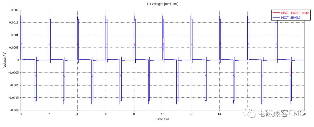
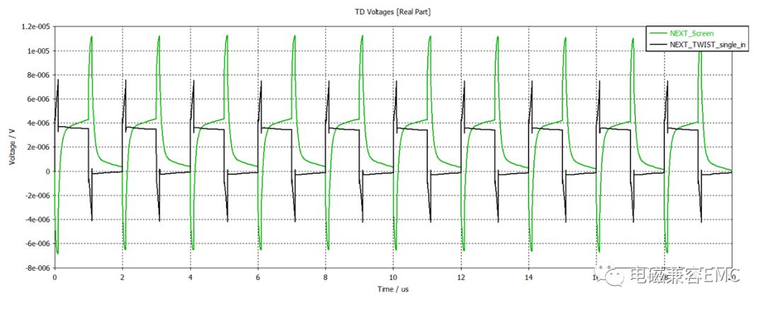
Fig59.å•çº¿åŒç»žåŽè¿‘端噪声电压波形
结论:线æŸè®¾è®¡ä¸çš„串扰与线æŸçš„布局和处ç†æ–¹å¼ç›¸å…³ï¼Œæ¡ä»¶å…许情况下,线æŸåº”该尽é‡å•ç‹¬å±è”½å¤„ç†ï¼Œè‹¥äº§å“æˆæœ¬ä¸å…许,也å¯ä»¥é€šè¿‡åŒç»žç‰æ–¹å¼å¯¹çº¿æŸå¤„ç†ï¼Œä»Žè€Œé™ä½Žä¸²æ‰°å¯èƒ½é€ æˆçš„å½±å“。对于有å¤æ‚线æŸè¦æ±‚的设计,需è¦æ…Žé‡è€ƒè™‘线æŸé—´çš„串扰å¯èƒ½é€ æˆçš„å½±å“,这个串扰既有å¯èƒ½å˜åœ¨äºŽåŒä¸€çº¿æŸå†…,也å¯èƒ½å˜åœ¨äºŽä¸åŒçº¿æŸé—´ã€‚
Fine Steel Cord For PU Timing Belts
Fine Steel Cord For PU Timing Belts
PU Timing Belts with steel cord, Timing belts truly endless or Jointed endless with cleats, for conveyor and Transmission Purpose
Our firm is providing an extensive series of PU Timing Belt with Steel Cord. Professionals use top quality material, which is sourced from truthful sellers of market to make this product. Our clientele can attain this product in varied specifications that meet on their necessities. Quality checkers also check this product on definite quality standards before delivery to the patrons.
Fine Steel Cord,Fine Steel Wire Rope,Pu Belt Steel Cord,Pu Timing Belt With Steel Cord
ROYAL RANGE INTERNATIONAL TRADING CO., LTD , https://www.royalrangelgs.com